Panel display having precise location trap anode array strcture and its manufacturing technology

A technology of flat panel display and array structure, which is applied in cold cathode manufacturing, electrode system manufacturing, discharge tube/lamp manufacturing, etc. It can solve the problems of no more effective solution, improve the production success rate, and improve display resolution. The effect of efficiency and simplification of the manufacturing process

Inactive Publication Date: 2006-06-28
ZHONGYUAN ENGINEERING COLLEGE
View PDF0 Cites 6 Cited by
  • Summary
  • Abstract
  • Description
  • Claims
  • Application Information

AI Technical Summary

Problems solved by technology

For the above problems, there is no more effective solution in the current device structure and manufacturing process.

Method used


Image

  • Panel display having precise location trap anode array strcture and its manufacturing technology
  • Panel display having precise location trap anode array strcture and its manufacturing technology
  • Panel display having precise location trap anode array strcture and its manufacturing technology

Examples


Embodiment Construction

[0047] The present invention will be further described below in conjunction with the accompanying drawings and embodiments, but the present invention is not limited to these embodiments.

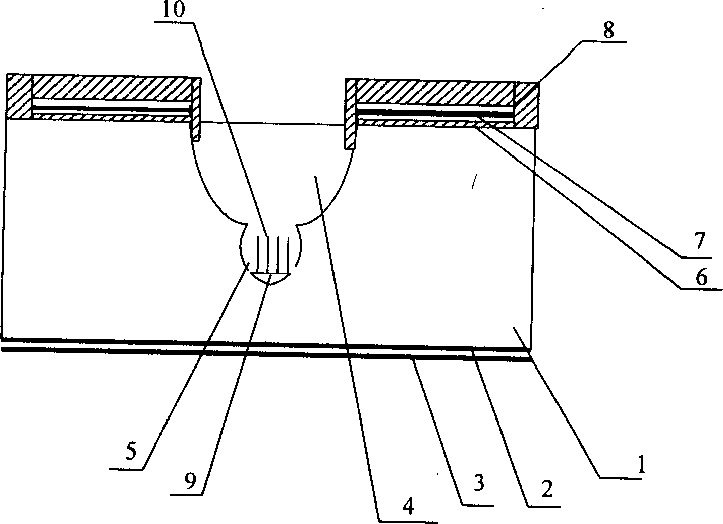
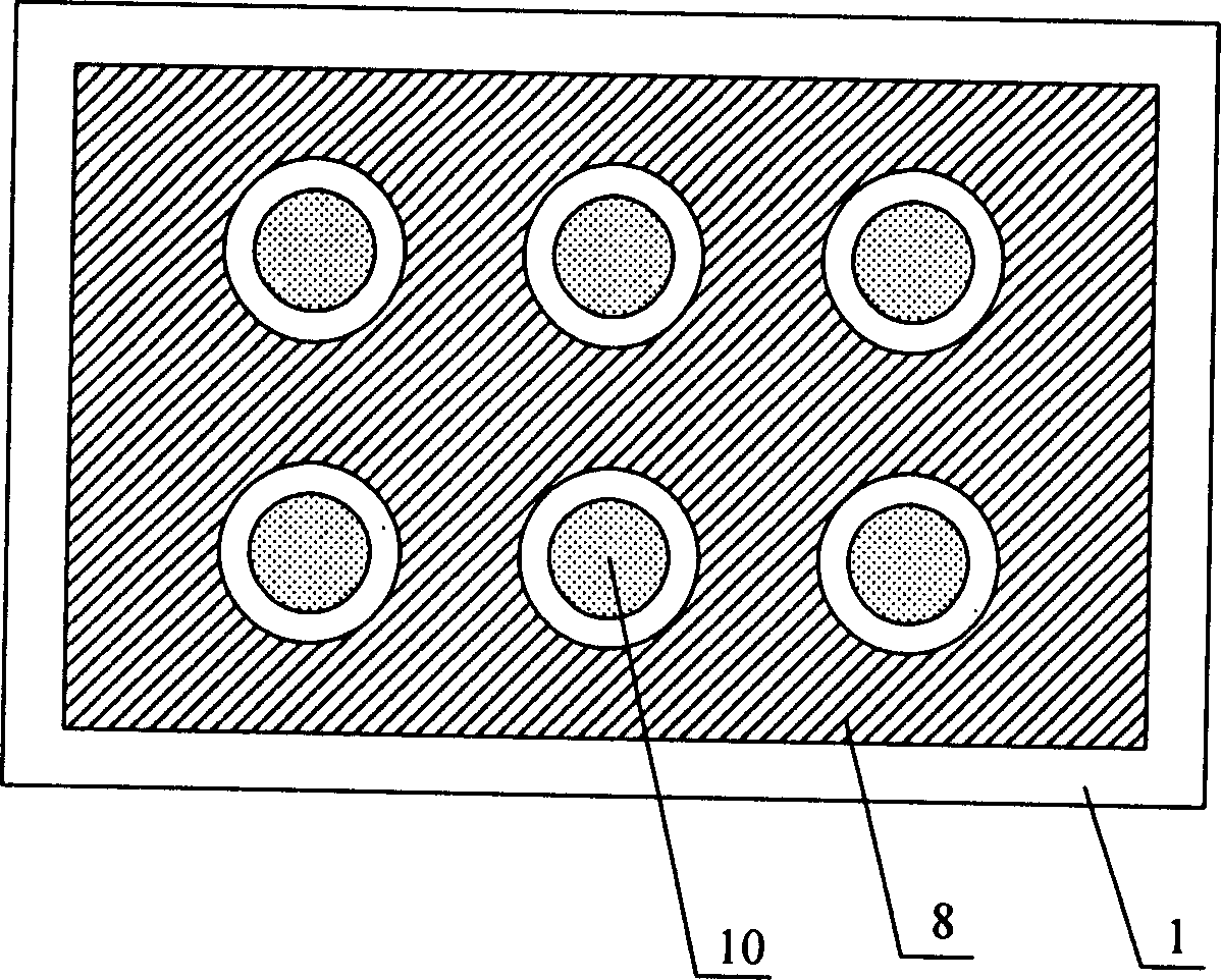
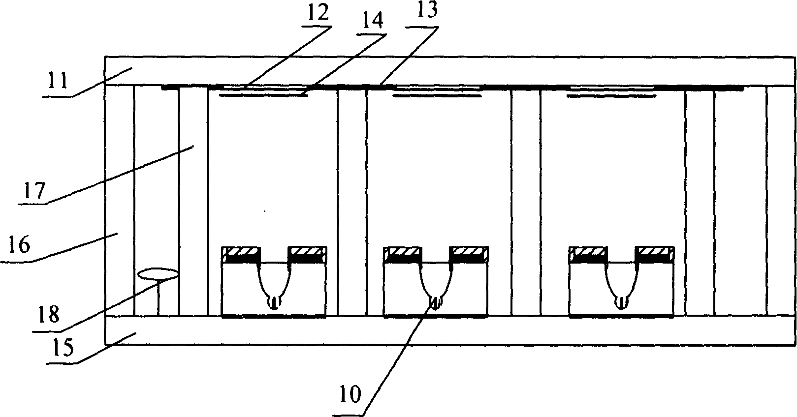
[0048] The present invention comprises a sealed vacuum chamber formed by a cathode panel 15, an anode panel 11 and surrounding glass enclosures 16; on the anode panel 11 there is a photoetched anode conductive layer 12 and a phosphor layer 14 prepared on the anode conductive layer 12 ; The supporting wall structure 17 and the accessory element 18 of the getter are fabricated on the cathode panel 15] with a precisely positioned well cathode array structure.

[0049] The precisely positioned well cathode array structure includes the substrate material silicon wafer 1, a layer of cathode conductive layer 2 evaporated on the lower surface of the substrate material silicon wafer, the cathode conductive layer 2 is covered with a cathode covering layer 3, and the substrate The material silicon wafe...


PUM


Abstract

This invention relates to a panel display with an accurate location trap cathode array structure and its process method, in which, said display includes a sealed vacuum cavity composed of a cathode panel, an anode panel and surrounding glasses, a photoetched anode conduction layer on the anode panel and a fluorescence powder layer on the anode conduction layer, a supporting wall structure and getters, an accurate location trap cathode array structure prepared on the cathode panel capable of determining the growing position of the carbon nm tube cathode and controlling its location, length and number and integrating with the control grating to reduce distances between them and avoid short circuit.

Description

technical field [0001] The invention belongs to the fields of plane display technology, microelectronic science and technology, vacuum science and technology, and nano science and technology, and relates to the manufacture of flat panel field emission displays, in particular to flat panels for carbon nanotube cathodes. The device manufacturing aspect of the field emission display particularly relates to the manufacturing process of the field emission flat display device of the carbon nanotube cathode with a precisely positioned well cathode array structure. Background technique [0002] In recent years, flat panel displays have been widely recognized for their advantages of high definition, flat panel, high image quality, light weight, and thin profile, and their application range has become wider and wider. The field emission flat panel display device made of carbon nanotubes as the cathode material is an emerging planar device. In addition to the common characteristics of ...

Claims


Application Information

Patent Timeline
Patent Type & Authority Applications(China)
IPC IPC(8): H01J29/02H01J9/00H01J29/04H01J31/12
Inventor 李玉魁
Owner ZHONGYUAN ENGINEERING COLLEGE
Why Eureka
Try Eureka