Supercharge Your Innovation With Domain-Expert AI Agents!

Organic electroluminescent display panel

一种电致发光显示、显示板的技术,应用在视频显示器领域,能够解决减小显示像素孔径比、面积增大等问题

Inactive Publication Date: 2005-06-08
SAMSUNG DISPLAY CO LTD
View PDF1 Cites 1 Cited by
  • Summary
  • Abstract
  • Description
  • Claims
  • Application Information

AI Technical Summary

Problems solved by technology

[0012] However, the above arrangement has a problem in that the display pixels are reduced due to the increase in the area of ​​the gate line for coupling the drain of the precharge transistor, the gate of the drive transistor, and the gate of the compensation transistor. Aperture ratio of

Method used


Image

  • Organic electroluminescent display panel
  • Organic electroluminescent display panel
  • Organic electroluminescent display panel

Examples


Embodiment Construction

[0033] In the following detailed description, only certain exemplary embodiments of the present invention are shown and described by way of illustration. As those skilled in the art would realize, the described embodiments may be modified in various different ways, all without departing from the spirit or scope of the present invention. The drawings and descriptions are therefore only schematic in nature and not restrictive.

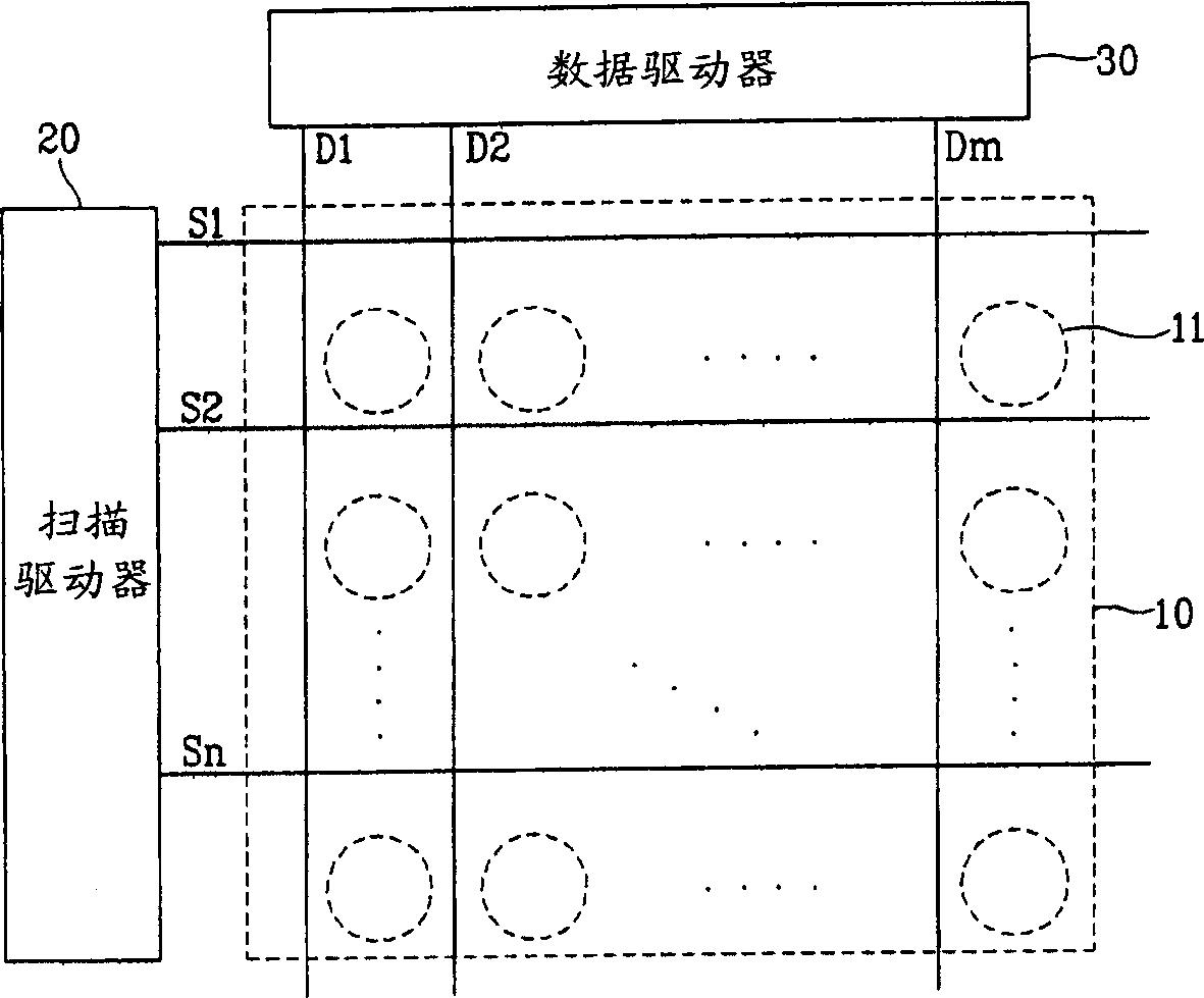
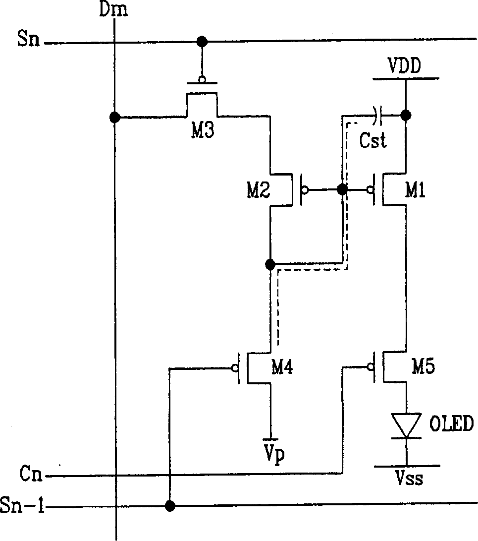
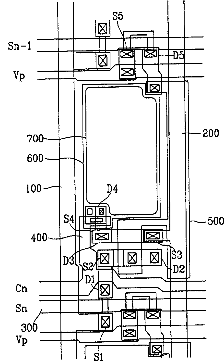
[0034] exist figure 2In order to simplify the description, it is shown that it is coupled to the mth data line D m and the nth scan line S n pixel circuit. Regarding the definition of scan lines, a scan line transmitting a current selection signal is referred to as a "current scan line", and a scan line transmitting a selection signal before the current selection signal is transmitted is referred to as a "previous scan line".

[0035] like figure 2 As shown, the pixel circuit 11 includes an organic EL element (OLED), transistors M1-M5 and a capaci...


PUM


Abstract

Provided is an organic EL display panel including display pixels with an improved aperture ratio. The display pixel includes a control electrode line coupled to the control electrodes of the first and second transistors and the main electrode of the fourth transistor, and a power electrode line substantially parallel to the data line and coupled to the main electrode of the first transistor. Channels of the first and second transistors are formed substantially parallel to the scan lines. A node of a control electrode line for coupling the control electrodes of the first and second transistors is arranged in a direction substantially perpendicular to the scanning line direction, and a part of the control electrode line extending to the main electrode of the fourth transistor is arranged in a substantially vertical direction. It is formed substantially parallel to the power supply electrode lines in a direction, and forms a capacitor together with the power supply electrode lines.

Description

technical field [0001] The present invention relates to a video display, and more precisely, the present invention relates to an organic electroluminescence (EL) display panel. Background technique [0002] In general, an organic EL display electrically excites a phosphorus organic compound to emit light. A light-emitting pixel consists of an anode (ITO), an organic thin film, and a cathode layer (metal). The organic thin film has a multilayer structure that maintains the balance between electrons and holes and improves emission efficiency, and includes EML (Emission Layer), ETL (Electron Transport Layer), and HTL (Hole Transport Layer). Organic thin films also include EIL (Electron Injection Layer) and HIL (Hole Injection Layer). [0003] The organic emission units are arranged in an n×m matrix form to constitute an organic EL display panel driven by voltage or current to display video data. [0004] figure 1 A schematic diagram showing a general organic EL display. ...

Claims


Application Information

Patent Timeline
Patent Type & Authority Applications(China)
IPC IPC(8): G09G3/30G09G3/32H01L21/20H01L27/32H05B33/12H05B44/00
CPCG09G3/3233G09G2300/0819G09G2300/0842G09G2300/0861G09G2310/0251G09G2320/043H10K59/12G09G3/30
Inventor 金禁男李乙浩
Owner SAMSUNG DISPLAY CO LTD
Features
  • R&D
  • Intellectual Property
  • Life Sciences
  • Materials
  • Tech Scout
  • Unparalleled Data Quality
  • Higher Quality Content
  • 60% Fewer Hallucinations
Learn More