Method for manufacturing a semiconductor device

A semiconductor and device technology, which is applied in the field of manufacturing semiconductor devices, can solve the problems of shorter channel length, lower threshold voltage, and inability to effectively reduce junction leakage current, so as to achieve the effect of reducing junction leakage current

Inactive Publication Date: 2005-08-03
ELPIDA MEMORY INC
View PDF1 Cites 2 Cited by
  • Summary
  • Abstract
  • Description
  • Claims
  • Application Information

AI Technical Summary

Problems solved by technology

That is, if a high-temperature heat treatment for a long period of time sufficient to remove the number of crystal defects is performed after dopant implantation, the implanted dopant diffuses so much that the effective channel length becomes short, resulting in a decrease in threshold voltage
Therefore, the number of crystal defects cannot be sufficiently reduced, and therefore, the junction leakage current caused by these defects cannot be effectively reduced

Method used


Image

  • Method for manufacturing a semiconductor device
  • Method for manufacturing a semiconductor device
  • Method for manufacturing a semiconductor device

Examples


Embodiment Construction

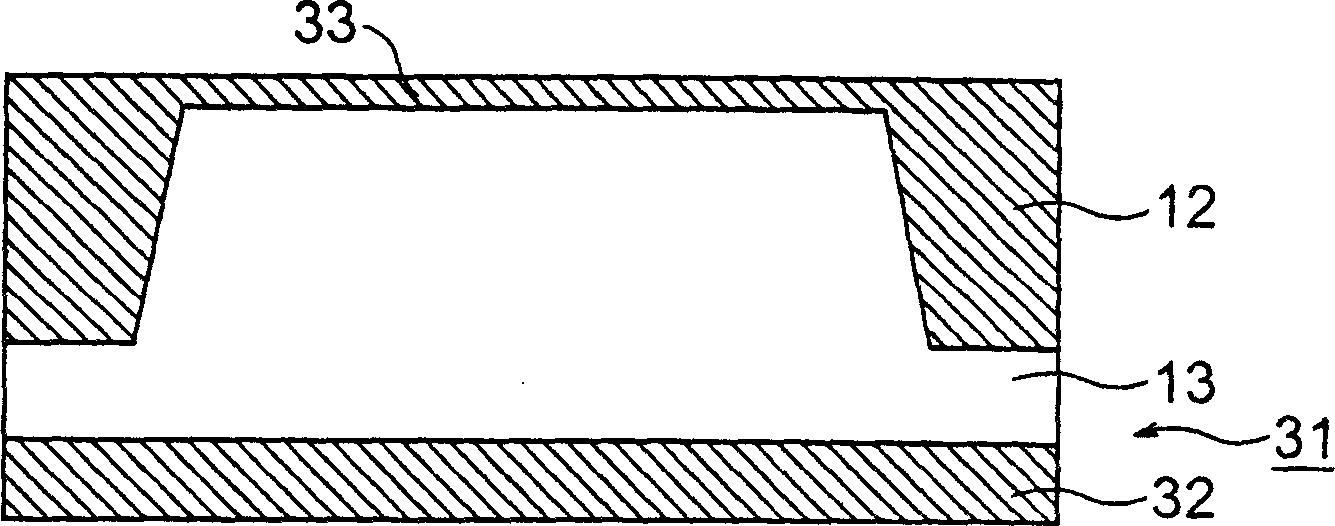
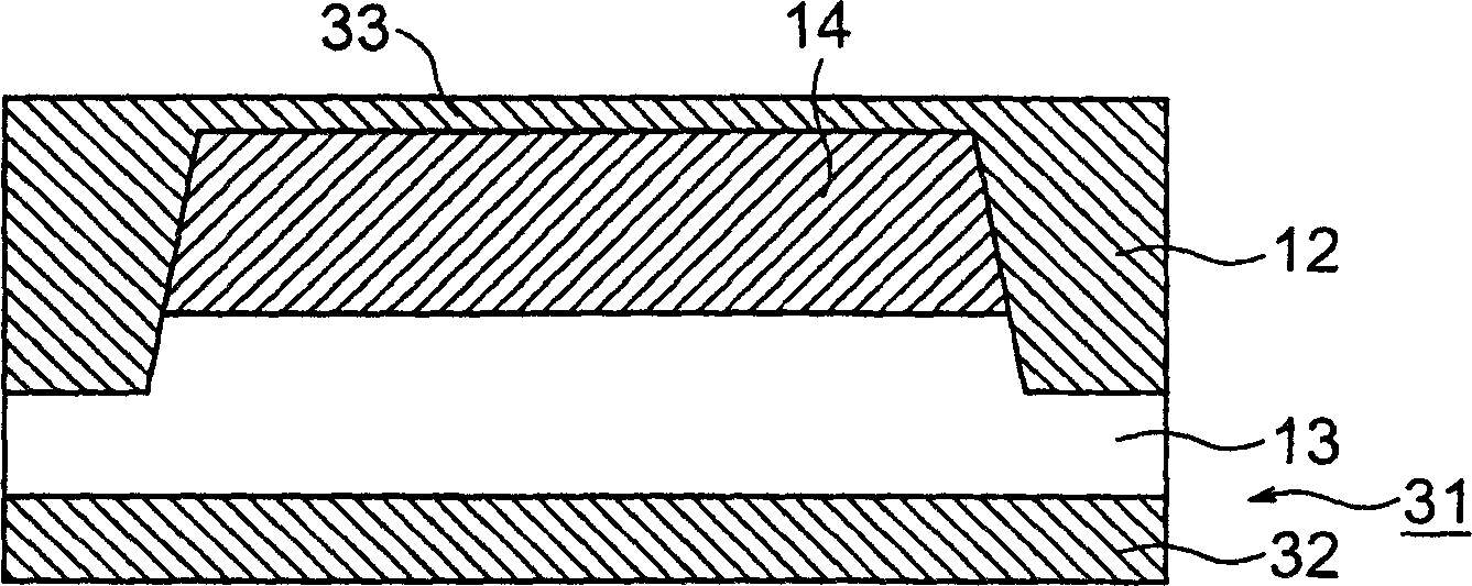
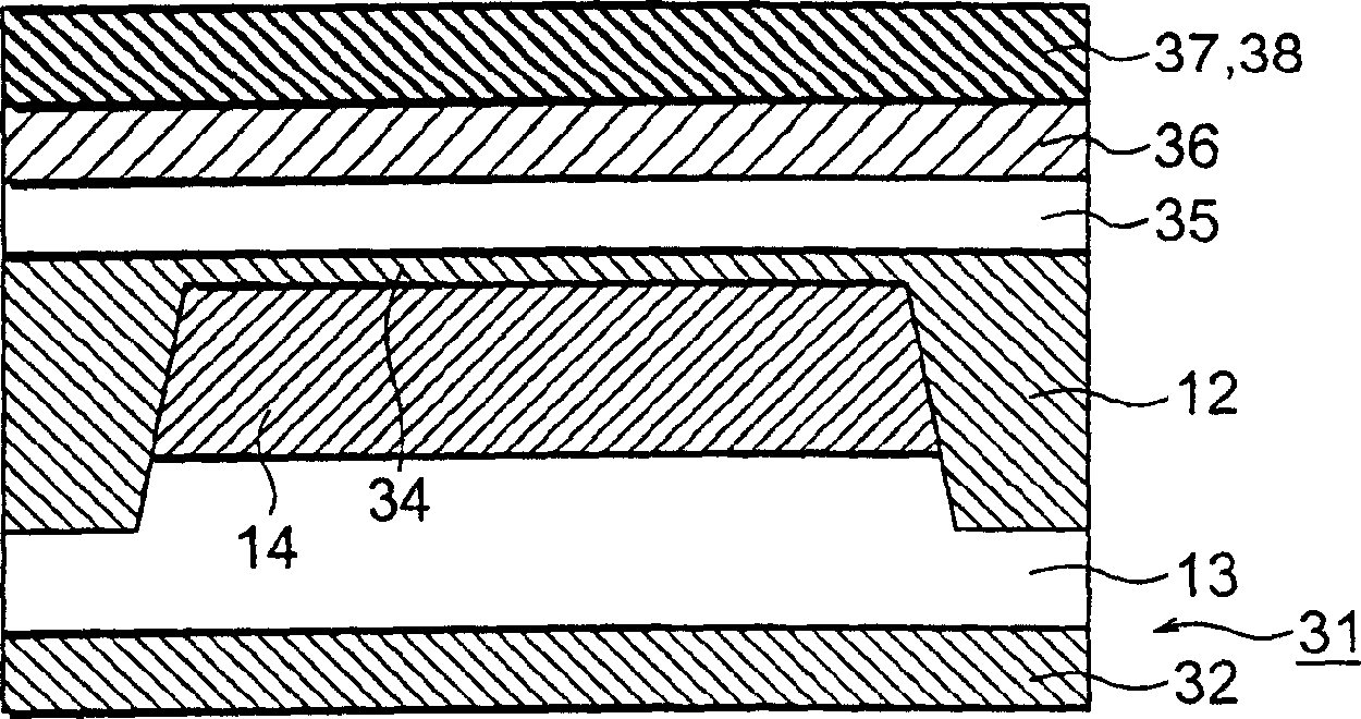
[0028]The present inventors conducted the following first and second experiments prior to the present invention. In the first experiment, a predetermined dose of dopant was implanted into the semiconductor substrate, and thereafter, heat treatment for redistributing the dopant was performed. By obtaining the relationship between the number of remaining defects and the amount of heat treatment, research was conducted on the number of crystal defects remaining after heat treatment. The term "amount of heat treatment" used herein means an amount approximated by the product of the time interval for performing the heat treatment and the temperature. A first experiment was performed while varying the dose of implanted dopants. It was thus found that the dependence of the number of defects remaining after heat treatment on the amount of heat treatment varies depending on the dose. Figure 8 shows the relationship between the normalized number of remaining defects and the normalized...


PUM


Abstract

A method for manufacturing a MOS transistors in a semiconductor device includes the step of implanting a dopant in a channel layer or source / drain regions by using a multi-step implantation and an associated multi-step heat treatment, wherein the multi-step implantation includes a number of steps of implantation each for implanting the dopant at a dosage lower than 1x10¹³ / cm2. The total dosage of the multi-step implantation ranges between 1x10¹³ / cm2 and 3x10¹³ / cm2.

Description

technical field [0001] The present invention relates to a method of manufacturing a semiconductor device, and more particularly, to a method of manufacturing a semiconductor device suitable for use in memory cells in DRAM devices, SEAM devices, etc. in mobile information terminals such as portable phones manufacture. Background technique [0002] Memory cells in DRAM or SRAM used in mobile information terminals particularly require MOS transistors that generate small junction leakage currents. Figure 10 The structure of a semiconductor device described in Patent Publication JP-A-2003-17586 is shown as an example of a conventional semiconductor device. [0003] In the semiconductor device 82, on the semiconductor substrate 31, a plurality of MOS transistors arranged in the form of transistor pairs sharing the bit line 11 are formed as shown in the drawing. The semiconductor substrate 31 has shallow trench isolation regions and active regions isolated from each other by the ...

Claims


Application Information

Patent Timeline
Patent Type & Authority Applications(China)
IPC IPC(8): H01L21/225H01L21/265H01L21/28H01L21/336H01L21/8238H01L21/8242H01L21/8244H01L27/092H01L27/108H01L27/11H01L29/78
CPCH01L21/823814H01L21/2253H01L21/823807H01L21/28061H01L29/6656H01L27/10873H01L21/2652H01L27/10811H01L21/823892H01L29/6659H01L21/2658H10B12/312H10B12/05H01L21/265
Inventor 小此木坚祐大汤静宪
Owner ELPIDA MEMORY INC
Why Eureka
Try Eureka