Photomask and method for repairing defects

A defect and photomask technology, applied in the field of photolithography, can solve the problems of reducing the transmission characteristics of photomasks, and achieve the effect of reducing risks and damages

Inactive Publication Date: 2005-09-21
DUPONT PHOTOMASKS
View PDF0 Cites 10 Cited by
  • Summary
  • Abstract
  • Description
  • Claims
  • Application Information

AI Technical Summary

Problems solved by technology

However, in photolithography systems using exposure wavelengths below about four hundred nanometers, substrate damage can lead to absorption of said exposure wavelengths, thus degrading the transmission characteristics of the associated photomask

Method used


Image

  • Photomask and method for repairing defects
  • Photomask and method for repairing defects
  • Photomask and method for repairing defects

Examples


Embodiment Construction

[0021] refer to Figures 1 to 3B To understand the preferred embodiment of the invention and its advantages, like reference numerals are used to designate like and corresponding parts.

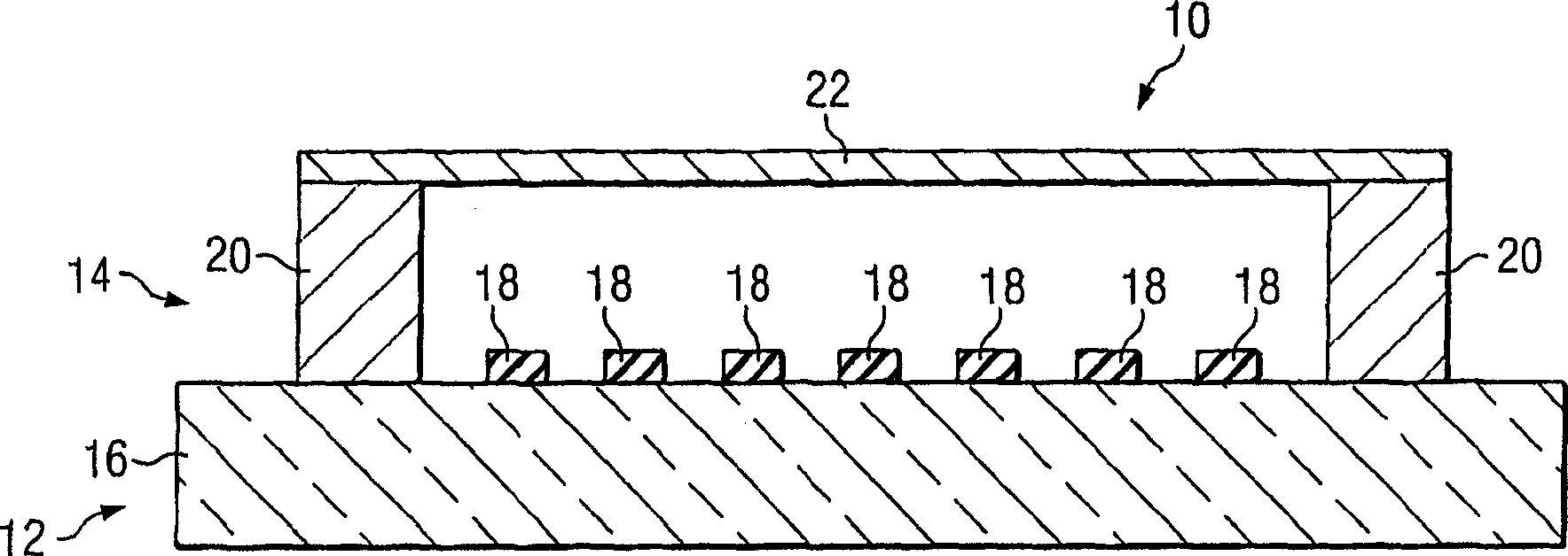
[0022] figure 1 A cross-sectional view of a photomask assembly 10 having a photomask 12 coupled to a pellicle assembly 14 is illustrated. Substrate 16 and patterned layer 18 cooperate with each other to form photomask 12, unlike known masks or reticles. Photomask 12 may have a variety of sizes and shapes including, but not limited to, circular, rectangular, or square. Photomask 12 may also be any of a variety of photomask types including, but not limited to, a one-time master, a five-inch reticle, a six-inch reticle, a nine-inch reticle, or any other An appropriately sized reticle, the photomask described above can be used to project an image of the circuit pattern onto a semiconductor wafer (not explicitly shown). Photomask 12 may also be a binary mask, a phase shift mask, an optical prox...


PUM


Abstract

A photomask and method for repairing defects on the same are disclosed. The photomask preferably includes a substrate, a buffer layer and a nontransmissive layer with the buffer layer disposed between the substrate and the nontransmissive layer. The method includes forming a pattern in the nontransmissive layer. If one or more defects are identified in the patterned nontransmissive layer, the buffer layer protects the substrate from damage when defects in the patterned nontransmissive layer are repaired.

Description

technical field [0001] The present invention generally relates to the technical field of photolithography, and more particularly, to a photomask and a method for repairing defects on the mask. Background technique [0002] Today's photolithography techniques often require short exposure wavelengths to successfully image very small-scale semiconductor devices on wafers. At wavelengths in or below the deep ultraviolet (DUV) range, for example below two hundred nanometers, materials and techniques commonly used to manufacture photomask components become increasingly important. [0003] A common method of making a photomask that involves imaging a circuit pattern in a resist layer, developing the resist layer, etching the resist layer and any uncovered areas of the opaque or semi-transmissive layer, and removing the remove the unetched portion of the resist layer. During this process, defects can arise if parts of the opaque or semi-transmissive layer remain on the substrate i...

Claims


Application Information

Patent Timeline
Patent Type & Authority Applications(China)
IPC IPC(8): G03F1/00H01L21/027
CPCG03F1/72
Inventor L·迪乌M·J·拉曼蒂亚
Owner DUPONT PHOTOMASKS
Why Eureka
Try Eureka