Non-volatile semiconductor memory device and writing method therefor

A non-volatile, semiconductor technology, applied in semiconductor devices, semiconductor/solid-state device manufacturing, static memory, etc., to achieve the effect of reducing data latch frequency and inspection frequency

Inactive Publication Date: 2005-09-28
PANASONIC CORP
View PDF5 Cites 7 Cited by
  • Summary
  • Abstract
  • Description
  • Claims
  • Application Information

AI Technical Summary

Problems solved by technology

[0018] The present invention solves the above problems, and its object is to provide a nonvolatile semiconductor memory device and a writing method thereof capable of performing data writing operations in a physical grid pattern, a logical grid pattern, etc. at high speed

Method used


Image

  • Non-volatile semiconductor memory device and writing method therefor
  • Non-volatile semiconductor memory device and writing method therefor
  • Non-volatile semiconductor memory device and writing method therefor

Examples


no. 1 example

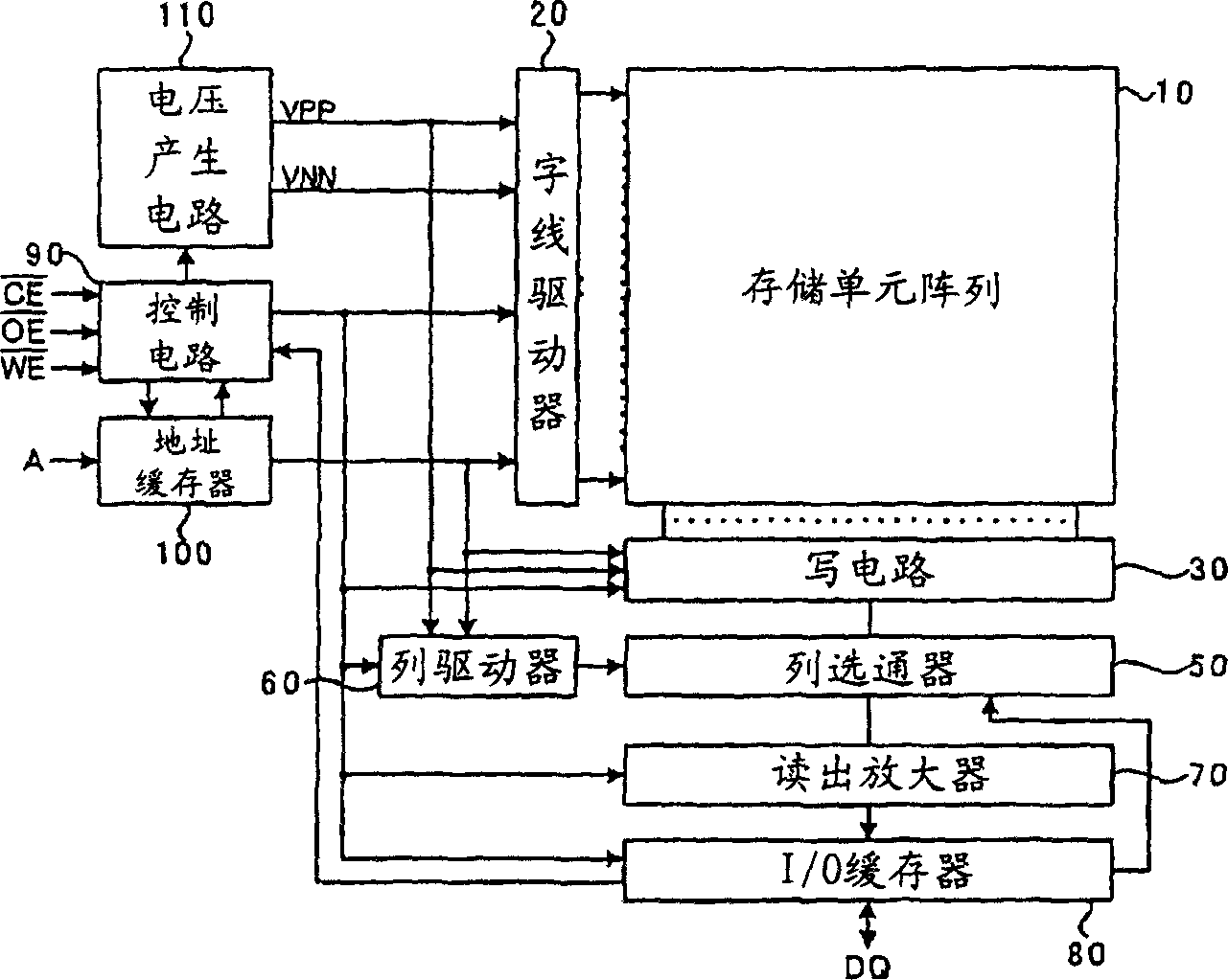
[0053] will refer to Figures 4 to 7 A flash memory (nonvolatile semiconductor memory device) according to a first embodiment of the present invention will be described in detail. Figure 4 is a configuration diagram showing a memory cell array and a write circuit of a flash memory (nonvolatile semiconductor memory device) according to the first embodiment. exist Figure 4 , denote with the same reference numerals as the Figure 15 The same constituent elements are shown in the background art, and a detailed description thereof is omitted. Only the different parts of the structure will be described below.

[0054] Figure 4 and showing background technology Figure 15 The difference between them lies in the structure of the word line driver and the write circuit. The single / multiple selection word line driver 21 selects one or two word lines and applies a predetermined voltage. The write circuits 30a to 30d are respectively connected to the bit lines BL0 to BL3, and each ...

no. 2 example

[0081] will refer to Figures 8 to 11 A flash memory (nonvolatile semiconductor memory device) according to a second embodiment of the present invention will be described in detail. The second embodiment improves the writing operation of the physical grid pattern of the first embodiment. According to the second embodiment, when the write operation of one of the two pages is completed according to the program operation and the simultaneous verify operation of the two pages but the write operation of the other page is not completed in the write operation, the new page and the page for which the write operation has not been completed are performed Write operations, and further increase the speed of data write operations.

[0082] Figure 8 is a configuration diagram showing a memory cell array and a write circuit of a flash memory (nonvolatile semiconductor memory device) according to a second embodiment of the present invention. exist Figure 8 In, the same reference numeral...

no. 3 example

[0102] will refer to Figures 12 to 14 A flash memory (nonvolatile semiconductor memory device) according to a third embodiment of the present invention will be described in detail.

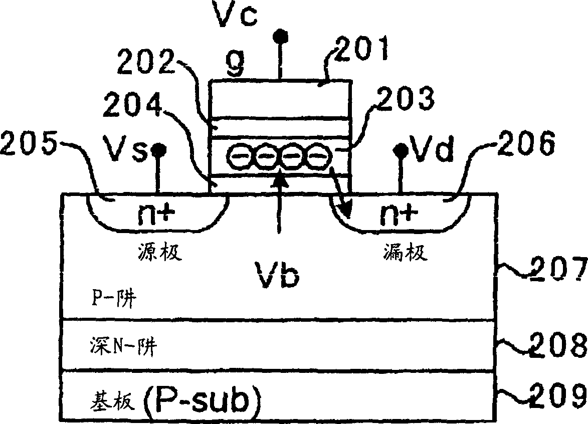
[0103] Figure 12 is a configuration diagram showing a memory cell array and a write circuit of a flash memory (nonvolatile semiconductor memory device) of a third embodiment. exist Figure 12 In, the same reference numerals are used to represent the Figure 8 The constituent elements of the second embodiment shown are constituent elements of the same function, and a detailed description thereof is omitted. Figure 12 with the second embodiment shown Figure 8 The difference is that a memory cell array 11 having a different structure is placed instead of the memory cell array 10, and a selection gate 25 and a single / multiple selection selection gate driver 26 are provided between the memory cell array 11 and the writing circuits 30a to 30d.

[0104] The memory cell array 11 is a NOR-type fla...


PUM


Abstract

The invention provided a nonvolatile semiconductor storage apparatus for speeding up the writing operation of a physical checker pattern, logical checker pattern, etc., which are performed in an inspection process. Writing circuits 30a, 30c of a 1st group connected to even-numbered bit lines BL0, BL2 and writing circuits 30b, 30d of a 2nd group connected to odd-numbered bit lines BL1, BL3 are controlled by control signals TSE, TSO respectively to the activated state and inactivated state. The writing operation of the physical checker pattern is carried out by; the program operation of a 1st page performed by setting a 1st word line and the writing circuits of the 1st group to the activated state; the program operation of a 2nd page performed by setting a 2nd word line and the writing circuits of the 2nd group to the activated state; and the simultaneous verify operation of the 1st and 2nd pages performed by setting the 1st, 2nd word lines and all writing circuits to the activated state.

Description

technical field [0001] The present invention relates to a nonvolatile semiconductor memory device in which data can be rewritable electrically, and more particularly to a nonvolatile semiconductor memory device in which a physical checker pattern, a logical checker pattern, etc. can be written at high speed. A volatile semiconductor memory device and a writing method thereof. Background technique [0002] Recently, nonvolatile semiconductor memory devices, especially flash memory, have been widely used in various fields because data is electrically rewritable in flash memory and data can be retained even when power is turned off. For example, they are used as memory devices for storing data in portable terminals such as cellular phones, digital cameras, silicon audio players, and the like. Furthermore, flash memory is also used as a rewritable program storage area in system LSIs such as microprocessors. [0003] In the inspection process of the flash memory, it is necessar...

Claims


Application Information

Patent Timeline
Patent Type & Authority Applications(China)
IPC IPC(8): G11C16/02G11C7/00G11C8/00G11C16/06G11C16/34G11C29/36H01L21/8247H01L27/10H01L27/115H01L29/788H01L29/792
CPCG11C16/3454G11C16/04G11C2029/3602G11C29/36
Inventor 河野和幸
Owner PANASONIC CORP
Why Eureka
Try Eureka