Semiconductor substrate, semiconductor circuits formed there and manufacture thereof

A semiconductor and carrier substrate technology, applied in semiconductor/solid-state device manufacturing, semiconductor devices, circuits, etc., can solve the problems that electricity is easily affected by the contact area and the difficulty of semiconductor circuits is high

Inactive Publication Date: 2005-10-12
INFINEON TECH AG
View PDF1 Cites 4 Cited by
  • Summary
  • Abstract
  • Description
  • Claims
  • Application Information

AI Technical Summary

Problems solved by technology

However, the disadvantage of this method is that it is difficult to connect the completed semiconductor circuit and its capacitance is easily affected by the contact area (contact-area-dependent)

Method used


Image

  • Semiconductor substrate, semiconductor circuits formed there and manufacture thereof
  • Semiconductor substrate, semiconductor circuits formed there and manufacture thereof
  • Semiconductor substrate, semiconductor circuits formed there and manufacture thereof

Examples


Embodiment Construction

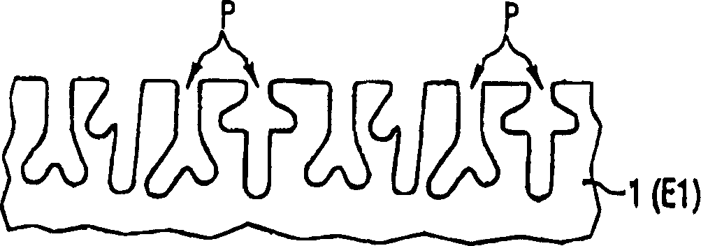
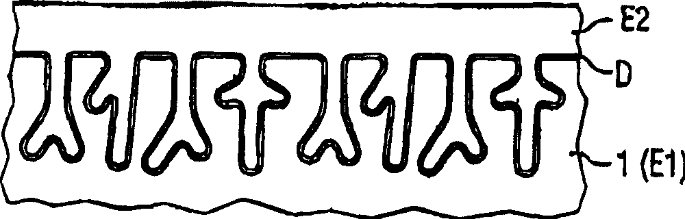
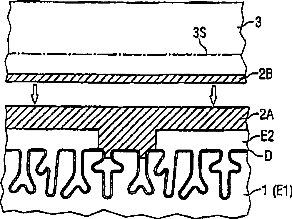
[0049] Figure 1A to Figure 1C It is a simplified cross-sectional view to illustrate the basic method steps of the semiconductor substrate manufacturing of the first embodiment of the present invention;

[0050] according to Figure 1A , multiple grooves P and a capacitor counter electrode E1 are formed in a carrier substrate 1, for example, it represents a semiconductor substrate, and preferably a silicon semiconductor wafer; preferably, multiple multiple pores P are formed to As the groove in the carrier substrate 1, it comprises n-doped silicon formed, for example, by electrochemical void etching, for example, the doping concentration of the carrier substrate is about 10 18 cm -3 , and first connected to a first voltage terminal and soaked in a hydrofluoric acid solution (25% by weight), while an electrode connected to a second voltage terminal is placed in the hydrofluoric acid solution. Then, generate a voltage of about 2 volts between the first voltage terminal and the...


PUM


Abstract

The invention relates to a semi-conductor substrate and a semi-conductor circuit embodied therein and a production method associated therewith. A plurality of cavities (P) provided with a respective dielectric layer (D) and a capacitor-electrode (E2) are embodied in order to produce capacitors buried in a carrier substrate and an actual semi-conductor component layer (3) is insulated from the carrier substrate (1) by an insulation layer (2).

Description

technical field [0001] The present invention relates to a semiconductor substrate, a semiconductor circuit formed therein and a manufacturing method thereof, in particular to a silicon-on-insulator (SOI) substrate containing various embedded capacitors. Background technique [0002] Since the integration density of semiconductor circuits, especially the storage density of DRAM (Dynamic Random Access Memories, DRAM), continues to increase, how to provide the required capacitance density on a smaller cell area becomes an issue. A problem to be faced. At present, the technologies related to the so-called trench capacitors and stack capacitors have made great progress. However, these process technologies will still face many limitations in the next generation of products. [0003] In addition, the integration of capacitors in logic and analog semiconductor circuits represents a considerable additional cost; since the current DRAM's highly optimized and highly space-saving cell-...

Claims


Application Information

Patent Timeline
Patent Type & Authority Applications(China)
IPC IPC(8): H01L21/02H01L21/334H01L21/84H01L27/12H01L29/94H10B12/00
CPCH01L28/82H01L27/1203H01L27/1087H01L27/10832H01L27/10867H01L29/66181H01L29/945H01L21/84H10B12/373H10B12/0385H10B12/0387
Inventor F·霍夫曼恩V·勒赫曼恩L·里斯奇W·雷斯纳M·斯佩奇特
Owner INFINEON TECH AG
Why Eureka
Try Eureka