
Optical type appearance testing method and optical type appearance testing device

An appearance inspection device and appearance inspection technology are applied in the fields of optics, measuring devices, and material analysis through optical means, which can solve problems such as the influence of inspection results, and achieve the effect of reducing false inspections and reducing costs

Inactive Publication Date: 2005-11-02
DAINIPPON SCREEN MTG CO LTD
View PDF2 Cites 11 Cited by
  • Summary
  • Abstract
  • Description
  • Claims
  • Application Information

AI Technical Summary

Problems solved by technology

However, in recent years, with the increase in the density of wiring on the substrate, this defect cannot be ignored.
In other words, in the substrate inspection device disclosed in the above-mentioned Japanese Patent Application Laid-Open No. 2002-76569, there is a possibility that the roller may cause fine scratches on the substrate, or that fine dust attached to the roller may adhere to the substrate. In the inspection of high-precision wiring, such fine scratches and debris will also have a bad influence on the inspection results.

Method used


Image

  • Optical type appearance testing method and optical type appearance testing device
  • Optical type appearance testing method and optical type appearance testing device
  • Optical type appearance testing method and optical type appearance testing device

Examples


Embodiment Construction

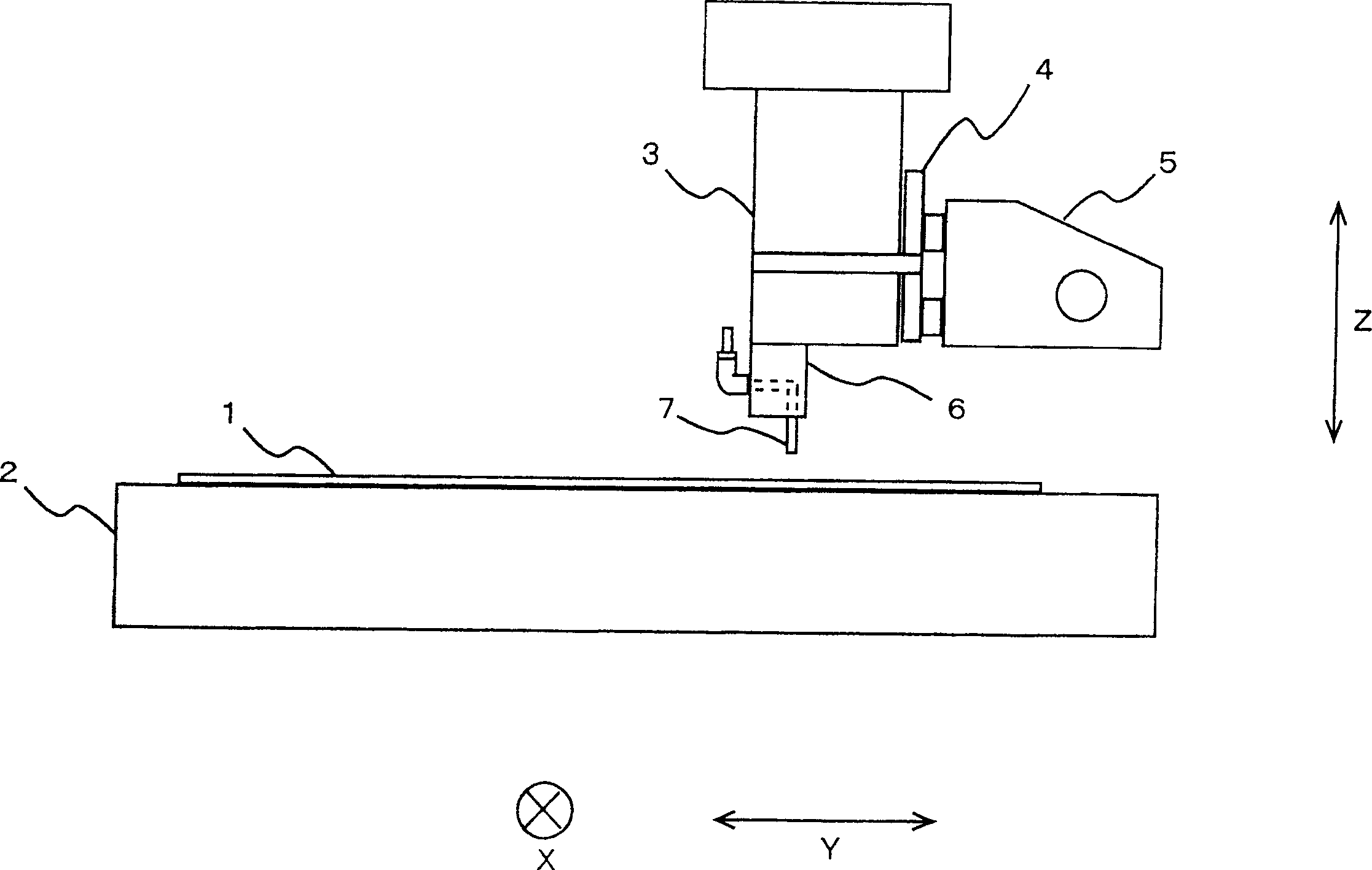
[0032]Embodiments of the present invention will be described below with reference to the drawings. Here, in order to make the description concrete, a case where a film mask on which a wiring pattern is formed is inspected will be described as an example. This example is not intended to limit the present invention. That is, the present invention is not limited to the inspection of thin film masks, but is also effective for inspection of flexible thin plate substrates.

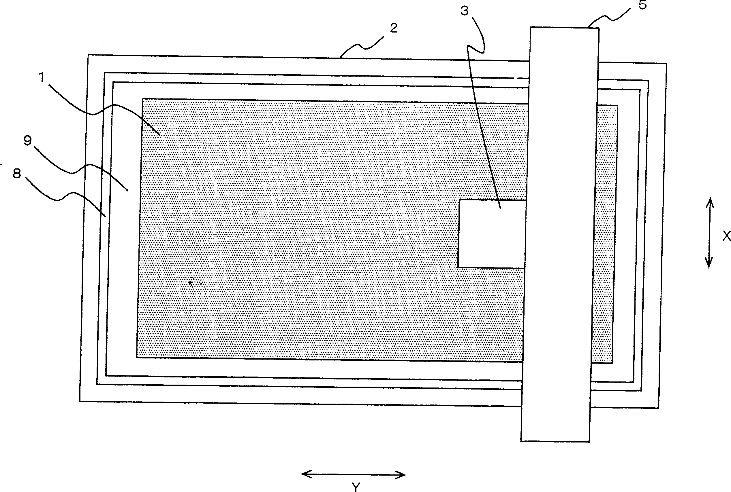
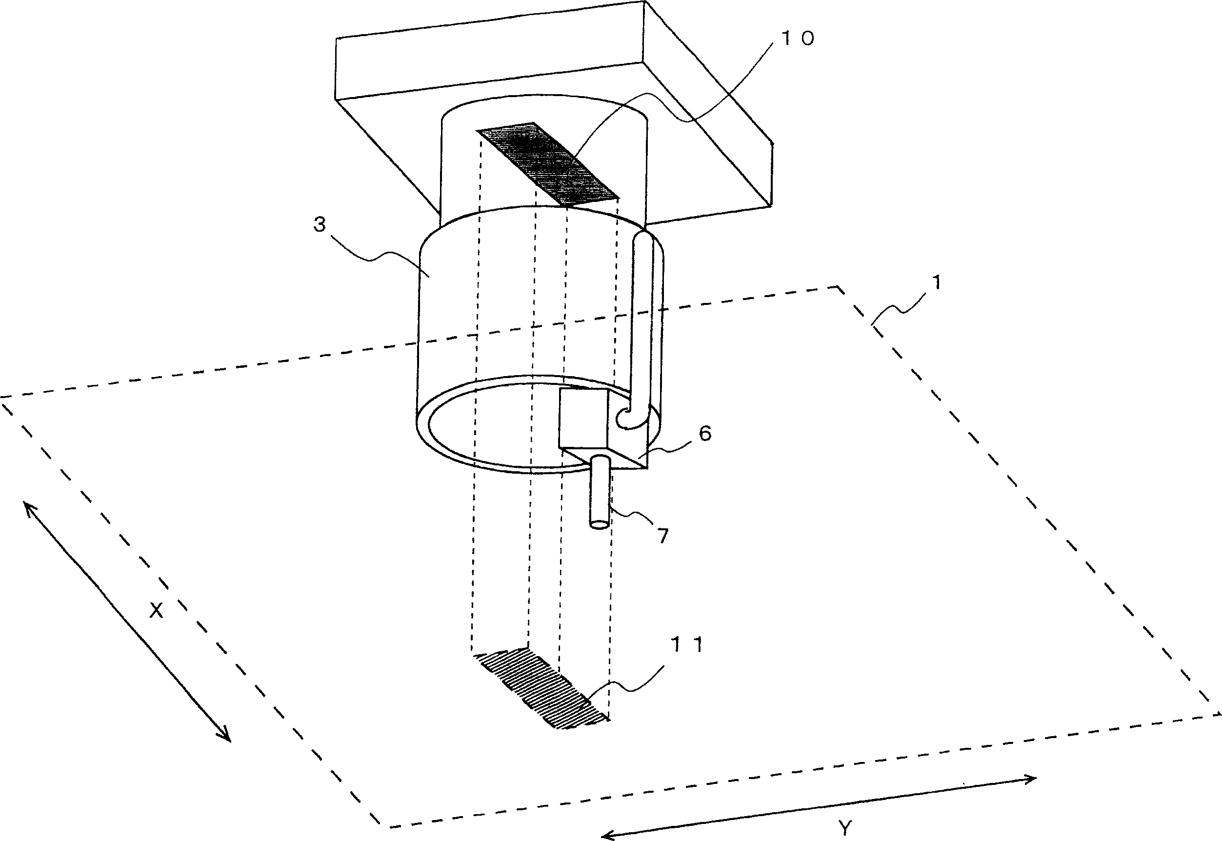
[0033] figure 1 It is a side view schematically showing the overall configuration of an optical visual inspection device according to an embodiment of the present invention. figure 2 is viewed from above the device figure 1 floor plan of the structure. figure 1 with figure 2 Among them, the optical appearance inspection device is composed of a stage 2 , an imaging unit 3 , a Z-axis base 4 , an X-axis base 5 , an air ejection member 6 , and a nozzle 7 .

[0034] figure 2 Among them, the stage 2 is forme...


PUM


Abstract

PROBLEM TO BE SOLVED: To accurately inspect a flexible thin substrate such as a film mask or the like using an inexpensive apparatus. ŽSOLUTION: The film mask 1 is placed on a placing table 2 and air is ejected to the vicinity of the scanning position of an imaging part 3 from an air blow block 6 attached so as to follow the imaging part 3 through a nozzle 7. The film mask 1 is scanned by the imaging part 3 while the periphery of the scanning position on the film mask 1 is closely brought into contact with the placing table 2 to photograph the inspection region of the film mask 1. Ž

Description

technical field [0001] The present invention relates to an optical appearance inspection method and an optical appearance inspection device, and more particularly to an optical appearance inspection method and an optical appearance inspection device for inspecting flexible thin substrates such as printed boards and film masks. Background technique [0002] It is well known that conductor wiring necessary for constituting a predetermined circuit is formed in a pattern on the surface of a printed circuit board on which electronic components and the like are mounted. On the other hand, the inspection of whether there is a defect in the wiring pattern of the printed circuit board or the like can be performed, for example, as follows. First, the printed circuit board is placed on the stage with the surface on which the pattern to be inspected is formed as the upper side. A photographing camera such as a CCD (Charge Coupled Device: Charged Coupled Device) camera is disposed above...

Claims


Application Information

Patent Timeline
IPC IPC(8): G01N21/956G03F1/84
CPCB07C5/3422G01N21/8806G01N21/95692G01N2021/5957G06T7/0008
Inventor 山本正昭小堀由高
Owner DAINIPPON SCREEN MTG CO LTD
Learn More