Interference scanning device and method

A technology for scanning devices and reference directions, applied in measuring devices, optics, instruments, etc., can solve problems such as time-consuming measurement, uncertain manufacturing process, and delayed product shipment speed, so as to improve scanning speed and accuracy and increase scanning area effect

Inactive Publication Date: 2005-12-07
CHROMA ATE
View PDF0 Cites 4 Cited by
  • Summary
  • Abstract
  • Description
  • Claims
  • Application Information

AI Technical Summary

Problems solved by technology

[0005] However, as mentioned above, because each detection can only be measured for the area covered by the object beam 300, and each measurement needs to wait for the mechanical lifting of the interferometer 8, so it takes a lot of time to measure each area to be measured. considerable time
When the area of ​​the object to be measured is large and cannot be fully covered by a single object beam 300, it is necessary to measure in different areas; especially if the area covered by the object beam 300 is much smaller than the size of the object to be measured, such as the current glass substrate for liquid crystal displays, if it is true Detecting the height of its surface topography area by area will inevitably seriously delay the speed of product shipment
[0006] Therefore, the current actual detection process is only as follows Figure 4 As shown, detection is performed at a few specific positions 71 on the surface 70 of the entire glass substrate 7 (marked by dotted lines). As for areas outside the area 71 marked by dotted lines, a small number of data are used to estimate, resulting in great uncertainty in the manufacturing process. , which greatly affects the quality

Method used


Image

  • Interference scanning device and method
  • Interference scanning device and method
  • Interference scanning device and method

Examples


Embodiment Construction

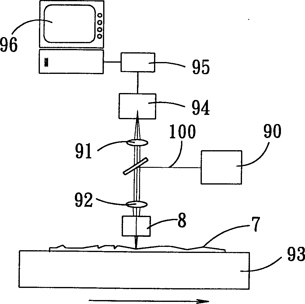
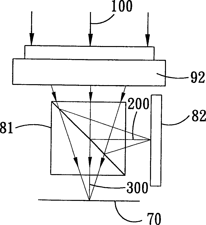
[0028] The foregoing and other technical contents, features and effects of the present invention will be clearly presented in the following detailed description of a preferred embodiment with reference to the drawings. All structures that are the same as those in the prior art are marked with the same reference numerals, and for the convenience of description, the structural ratio of the reflector will be exaggeratedly enlarged in the diagram.

[0029] The interference scanning device of the present invention can adopt the same white light source as the prior art, and also needs to place the object to be measured on a stage, so the overall scanning device of the present invention can be roughly referred to figure 1 as shown, Figure 5 In , only the interference unit where the structural features are located is enlarged and drawn. And in this example, it is taken as an example that the stage (not shown) can move along the left and right directions in the figure.
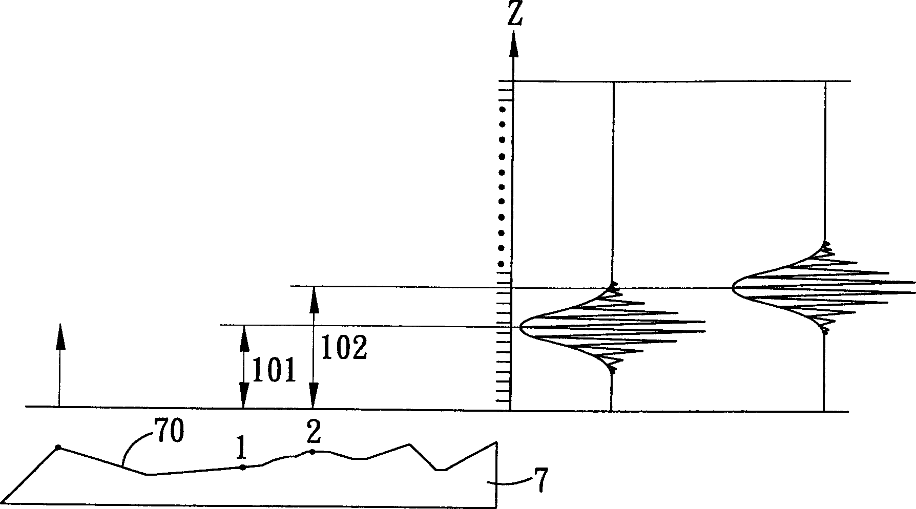
[0030] Fi...


PUM

PropertyMeasurementUnit
sizeaaaaaaaaaa

Abstract

This invention discloses a interference scanning device, which is an improved structure on the basis of a reflector, the individual zones of the reflector have different optical paths and each zone gets its own optical path interference information of every instant and sums up the information to find out the instant information specific being tested positions with the help of computing the moving rate of the interfere unit to simulate the up-down measurement to said positions. Each time when measuring, the interference scan device only needs to shift the interfere unit horizontally at the same height to obtain the measured result of the interferometer.

Description

technical field [0001] The present invention relates to an interference scanning device and method, in particular to a profile scanning device and method that uses a step-shaped lens to generate an optical path difference to achieve the optical path change effect of an interferometer. Background technique [0002] With the advancement of technology and the improvement of manufacturing process, the line width of semiconductor, flat panel display, micro-electromechanical, optical communication and other fields has been decreasing year by year, and the number of components per unit volume has grown rapidly. Especially the application of nanotechnology has pushed the manufacturing process to a new level. Realm; as the size of the manufacturing process shrinks, it becomes more and more difficult to control the quality. Taking the thin film transistor-liquid crystal display manufacturing process as an example, the amount of liquid crystal in the manufacturing process is controlled ...

Claims


Application Information

Patent Timeline
Patent Type & Authority Applications(China)
IPC IPC(8): G02B26/10
Inventor 林耀明
Owner CHROMA ATE
Why Eureka
Try Eureka