Laser-assisted in-situ mass transfer method and system

A laser-assisted transfer method technology, applied in laser welding equipment, welding equipment, metal processing equipment, etc., can solve problems such as yield and efficiency, increase transfer efficiency, improve processing yield, and avoid difficulties in optical path adjustment Effect

Active Publication Date: 2021-09-17
TSINGHUA UNIV
View PDF6 Cites 2 Cited by
  • Summary
  • Abstract
  • Description
  • Claims
  • Application Information

AI Technical Summary

Problems solved by technology

[0006] In order to solve the problems of yield and efficiency in the existing mass transfer link, the present invention provides a laser-assisted in-situ mass transfer method and system

Method used


Image

  • Laser-assisted in-situ mass transfer method and system
  • Laser-assisted in-situ mass transfer method and system
  • Laser-assisted in-situ mass transfer method and system

Examples


Embodiment Construction

[0029] In order to make the purpose, technical solutions and advantages of the embodiments of the present invention clearer, the technical solutions in the embodiments of the present invention will be clearly and completely described below in conjunction with the drawings in the embodiments of the present invention. Obviously, the described embodiments It is a part of embodiments of the present invention, but not all embodiments. It should be understood that the specific embodiments described here are only used to explain the present invention, not to limit the present invention. Based on the embodiments of the present invention, all other embodiments obtained by persons of ordinary skill in the art without making creative efforts belong to the protection scope of the present invention.

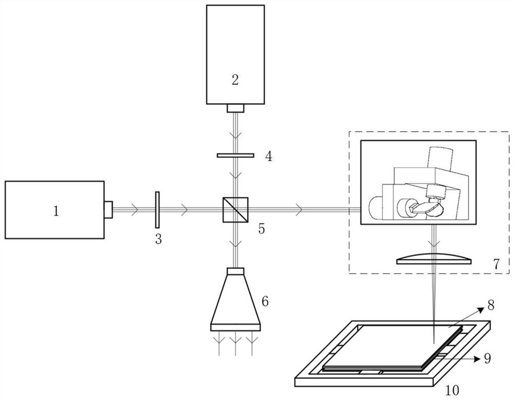
[0030] Such as Figure 1-Figure 6 As shown, a laser-assisted in-situ mass transfer method includes the following steps:

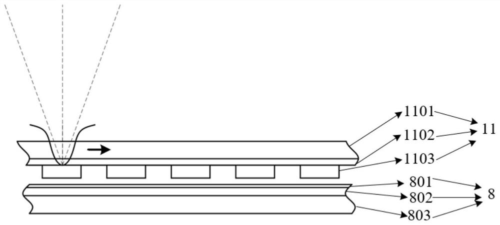
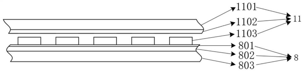
[0031] S1. Prepare the substrate 11 on which the Micro-LED chip 110...


PUM


Abstract

The invention discloses a laser-assisted in-situ mass transfer method and system. The method mainly comprises the following steps: scanning a GaN/sapphire substrate on which Micro-LED chips grow through a laser galvanometer according to the characteristics that the wavelength of infrared laser is longer, and the radius of laser spots is larger on the premise of guaranteeing the energy density of laser, and stripping the Micro-LED chips from the substrate and transferring the Micro-LED chip to a temporary transfer structure; carrying out point-by-point rapid scanning on a temporary transfer structure by using the laser galvanometer according to the cold processing effect of ultra-short pulse laser and the energy accumulation principle of multi-pulse action to realize high-speed fixed-point mass transfer of Micro-LED chips to a target substrate; and introducing two kinds of laser into the same laser processing light path through a half-reflecting mirror, and arranging a laser beam expanding device at an unused laser light outlet. Mass transfer of the Micro-LED chips is carried out by adopting double-laser-beam scanning and pulse laser point-by-point scanning, the transfer rate is high, and the yield is ensured.

Description

technical field [0001] The invention belongs to the field of semiconductor optoelectronic technology, in particular to a laser-assisted in-situ mass transfer method and system. Background technique [0002] Micro-LED is a micro-light-emitting diode, which refers to a high-density integrated LED array, in which the distance between LED pixels in the array is on the order of 10 μm, and each LED pixel can emit light by itself. Compared with LCD and OLED technologies, Micro-LED has become a recognized next-generation display technology in the industry due to its high resolution, low power consumption, high brightness, high color saturation, fast response, thin thickness, and long life. [0003] The Micro-LED manufacturing process mainly includes four key technologies, namely epitaxy and chip technology, mass transfer technology, bonding technology, and colorization scheme. Among them, the mass transfer technology mainly refers to the technology of quickly and accurately transfe...

Claims


Application Information

Patent Timeline
Patent Type & Authority Applications(China)
IPC IPC(8): B23K26/064B23K26/0622B23K26/082B23K26/70
CPCB23K26/0643B23K26/0624B23K26/082B23K26/702
Inventor 张震杨伟刘义杰
Owner TSINGHUA UNIV
Why Eureka
Try Eureka