Circuit simulation method, device model, and simulation circuit

A circuit simulation and device model technology, which is applied to circuits, electrical components, semiconductor devices, etc., can solve problems such as heat exchange of components in the circuit, increase in processing time, and deterioration of circuit simulation accuracy, and achieve high-efficiency circuit simulation. Effect

Inactive Publication Date: 2005-12-14
PANASONIC CORP
View PDF1 Cites 8 Cited by
  • Summary
  • Abstract
  • Description
  • Claims
  • Application Information

AI Technical Summary

Problems solved by technology

[0014] However, according to the method of the above-mentioned prior art, for example, in the simulation of the transient response of the circuit, the method of Patent Document 1 and VBIC95 only considers the main cause of the temperature change, and does not consider the internal components of the circuit. heat exchange between
Therefore, the circuit simulation accuracy of the characteristics of the device having temperature dependence is deteriorated
[0015] In addition, in the method of Patent Document 1, it is necessary to repeatedly calculate the temperature when obtaining the state at each time, so the processing time is greatly increased compared with the conventional circuit simulation which does not consider the temperature change of the element in the past.

Method used


Image

  • Circuit simulation method, device model, and simulation circuit
  • Circuit simulation method, device model, and simulation circuit
  • Circuit simulation method, device model, and simulation circuit

Examples


Embodiment Construction

[0037] Embodiments of the present invention will be described below with reference to the drawings.

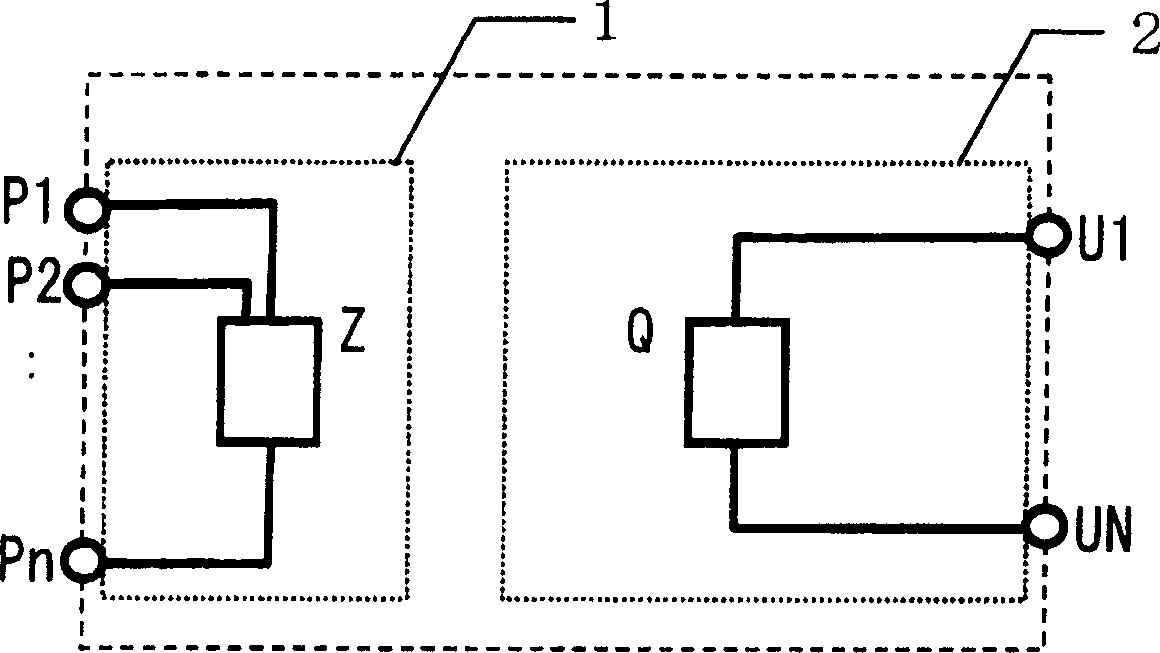
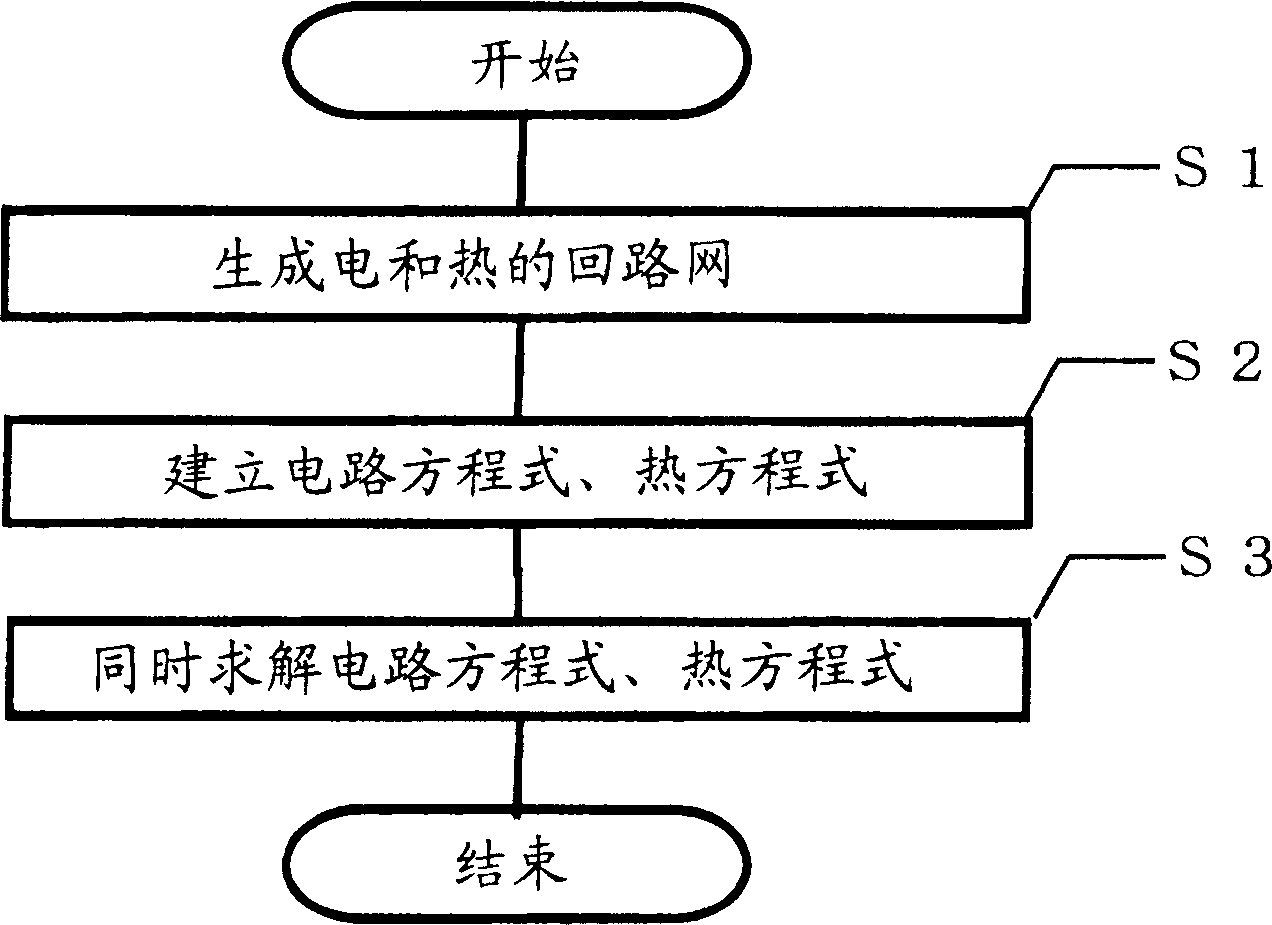
[0038] figure 1 is a schematic diagram of a device model for circuit simulation of the present invention, figure 2 is a flowchart showing the circuit simulation method of the present invention.

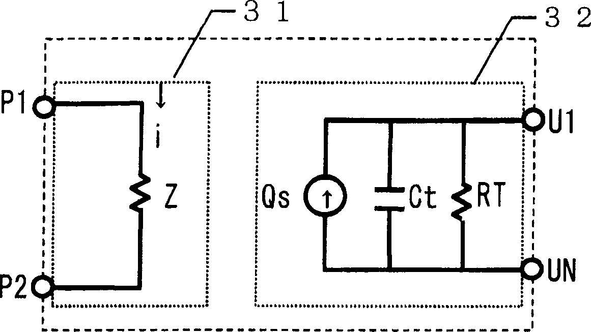
[0039] First, the outline thereof will be described. The device model used for circuit simulation of the present invention is as figure 1 What is shown is a model (hereinafter referred to as an electrothermal hybrid model) having both an electrical model 1 representing the electrical characteristics of an element and a thermal model 2 representing the thermal characteristics of the same element.

[0040] The electrical model 1 has terminals P1 to Pn corresponding to the number of devices, and the thermal model 2 has terminals (hereinafter referred to as thermal terminals) U1 and UN capable of exchanging heat between elements. Furthermore, the electrical characteristics of the e...


PUM


Abstract

A plurality of elements constituting a semiconductor integrated circuit to be designed are each converted to a device model which merges an electric model exhibiting electric characteristics of the element and a thermal model exhibiting thermal characteristics of the element, and a thermal resistor is inserted between the elements where heat exchange occurs, thereby electric and thermal circuits are formed. Then circuit and heat equations are formulated with respect to the electric and thermal circuits, and then the equations are solved together to acquire electric and thermal characteristics of each element in the circuit. As a result, it becomes possible to achieve high-precision device characteristics which precisely reflect the temperature variation of each element in the circuit during simulation.

Description

technical field [0001] The present invention relates to a circuit simulation method for evaluating circuit characteristics using a circuit simulator in the design of semiconductor integrated circuits, especially in circuit design engineering. In addition, device models and simulated circuits using the method are covered. Background technique [0002] In semiconductor integrated circuits (hereinafter referred to as ICs) that control devices that require high-current driving, such as motors and plasma displays, the temperature of the components that make up the IC or the entire IC may change dynamically during the simulation process due to self-heating, etc. Changes, and the possibility of IC characteristics changing is higher than other ICs. Therefore, it is necessary to grasp the acceptable temperature range of ICs or components and have sufficient countermeasures in circuit design. [0003] Circuit simulators are often used to evaluate circuit characteristics of ICs. As ...

Claims


Application Information

Patent Timeline
Patent Type & Authority Applications(China)
IPC IPC(8): G06F17/50H01L21/82H01L29/00
CPCG06F30/367
Inventor 米山慎一郎三岛英树
Owner PANASONIC CORP
Why Eureka
Try Eureka