
Folded-flex bondwire-less multichip power package

A technology of flexible substrates and assembly parts, which is applied in the field of multi-chip power modules, can solve the problems of expensive process, complex thermal channel design, reduce the high resistance effect of wire bonding, etc., achieve a wide heat dissipation area, improve heat dissipation, and increase heat dissipation channels Effect

Active Publication Date: 2010-10-13
INVENSAS CORP
View PDF6 Cites 0 Cited by
  • Summary
  • Abstract
  • Description
  • Claims
  • Application Information

AI Technical Summary

Problems solved by technology

Also, the complex lead connections and tight spacing requirements of these packages complicate the design of thermal vias on the board, which is important for proper thermal arrangement
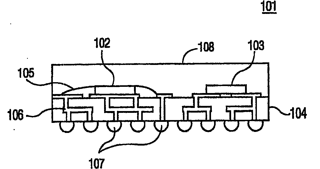
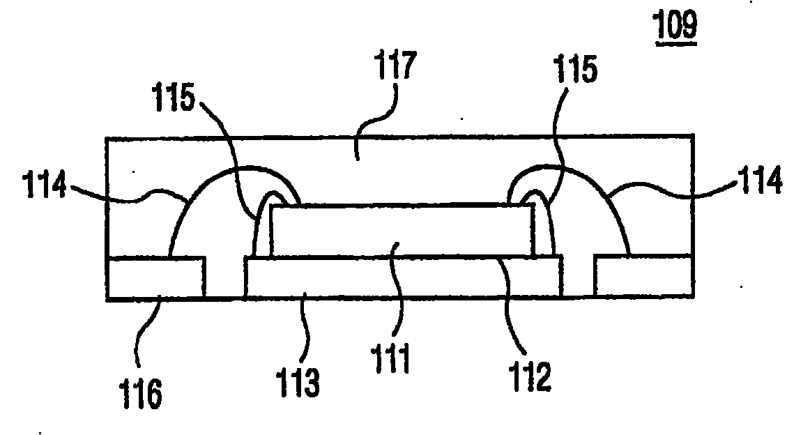
[0006] Both currently available commercial packages use multiple wire bonds per device and IC interconnects to reduce the high resistance effects of the wire bonds
But adding more parallel leads to lower the resistance eventually reaches the limit (2-3mΩ) and the process becomes very expensive

Method used


Image

  • Folded-flex bondwire-less multichip power package
  • Folded-flex bondwire-less multichip power package
  • Folded-flex bondwire-less multichip power package

Examples


Embodiment Construction

[0028] image 3 is an internal view of one embodiment of a folded flexible bondless leadless multi-chip power package in accordance with the present invention. Individual devices 301 , 301 ′, 301 ″, 301 ″′ etc. including semiconductor power dies as well as IC dies are attached to the main body portion 306 of the continuous flexible substrate 302 . Devices 301, 301', 301", 301"', etc. on the surface of each device die have device pads (not shown) with flip-chip bumps. Extended portions 303 and 303' of flexible substrate 302 are folded over devices 301 and 301' and devices 301" and 301"', respectively. This flexible substrate is equipped with copper contact pads on its bottom surface ( image 3 not visible in ) and connection 304 for attaching the circuit board. A molding compound is formed around the package in the shape 305 of an elongated rectangular box. A flexible substrate for semiconductor packaging is a stack of layers that typically includes a solder mask layer, a cop...


PUM


Abstract

A multichip wirebond-less integrated circuit and power die package is based on a folded single-layer flex circuit. The package is formed with metal-studbumped power dies and IC's flipchiped to a patterned flex substrate. Extensions of the flex substrate are folded and attached to the backside of the dies for electrical and / or thermal contact. I / O pins are along the periphery of the package for standard SMT mounting while heatspreaders are attached to both sides of the package for double-sided cooling.

Description

technical field [0001] The present invention relates to integrated power modules, and more particularly to folded, flexible, bond-wireless, multi-chip power modules for high power densities. Background technique [0002] Applications requiring high power conversion, such as microprocessors, automotive electronics, and voltage regulators for communications, have created a trend toward higher power density at lower cost. Therefore, in order to meet future power density requirements, integrated power module solutions are required instead of traditional discrete solutions. But the integration of power electronic components (such as devices, ICs, passive components, etc.) in the form of modules is complicated by the presence of a wide variety of materials in the modules. [0003] Only recently have two commercially available state-of-the-art multi-chip power packages for DC-DC power conversion provide an integrated system solution. The first commercially available packages for ...

Claims


Application Information

Patent Timeline
Patent Type & Authority Patents(China)
IPC IPC(8): H01L23/498H01L23/538
CPCH01L2224/48237H01L24/48H01L2924/01079H01L23/5387H01L2924/13091H01L2924/30107H01L2924/15747H01L2224/85447H01L2924/00015H01L2924/14H01L2924/181H01L2224/48257H01L2924/00014H01L2924/00H01L2224/05599H01L2224/45099H01L2924/00012H01L2224/45015H01L2924/207
Inventor S·哈奎G·布伦宁
Owner INVENSAS CORP
Learn More