
Flexible circuit substrate
A flexible circuit substrate, anisotropic technology, applied in the direction of circuit, printed circuit components, printed circuit structural connection, etc., can solve the problems of warpage, undulation, operation obstacles and other problems of flexible circuit substrate, and achieve the effect of good workability
- Summary
- Abstract
- Description
- Claims
- Application Information
AI Technical Summary
Problems solved by technology
Method used
Image

Examples
Embodiment 1
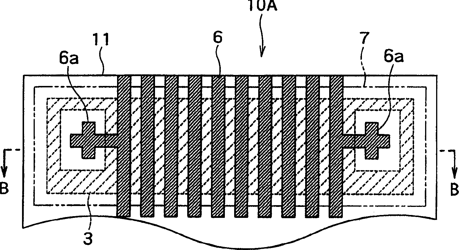
[0026] figure 1 It is a plan view of Embodiment 1 of the present invention, showing an end portion of a flexible circuit board provided with a connection terminal connected to a target device such as a display panel. exist figure 1 In the center of , 12 surface treatment layers (terminals) 6 are arranged at equal intervals along the longitudinal direction in the figure, and marks 6a extend from the left and right outermost terminals 6 .
[0027] Then, on the circuit board 10A, the anisotropic conductive resin layer 7 is formed on a region extending from the outer edge 11 of the board including the terminals 6 and the marks 6a to a little inside. For this reason, the filling amount of the anisotropic conductive resin must be appropriate and cannot be used too much.
[0028] In addition, in figure 1 In the diagram, the back rough wiring layer 3 on the back side of the circuit board 10A is indicated by dotted lines (contours) and hatched lines (copper foil). The outer edge...
PUM
 Abstract
Description
Claims
Application Information