Memory controller

A control device and memory technology, applied in memory systems, instruments, memory address/allocation/relocation, etc., can solve problems such as inability to access SDRAM808 useless cycles, increase in the number of cycles to access SDRAM808, and inability to access SDRAM, etc.

Inactive Publication Date: 2006-01-18
PANASONIC CORP
View PDF1 Cites 4 Cited by
  • Summary
  • Abstract
  • Description
  • Claims
  • Application Information

AI Technical Summary

Problems solved by technology

At this time, the address cannot be output to bank 1 until the precharge operation on bank 1 is completed.
That is, useless cycles in which SDRAM808 cannot be accessed
[0010] Also, in the conventional memory control device 801, when a write access to write data into the SDRAM 808 is performed after a read access to read data from the SDRAM 808, a useless cycle in which the SDRAM cannot be accessed is generated according to the specification of the SDRAM 808.
Therefore, there is a problem that when a plurality of components 804, 805, 806, and 807 request read access and subsequently request write access, the number of cycles to access the SDRAM 808 increases compared with the time of continuous write access and continuous read access.
If a refresh operation is performed after writing access requests from multiple components 804, 805, 806, 807, useless cycles may sometimes occur according to the SDRAM808 specification

Method used


Image

  • Memory controller
  • Memory controller
  • Memory controller

Examples


Embodiment approach 1

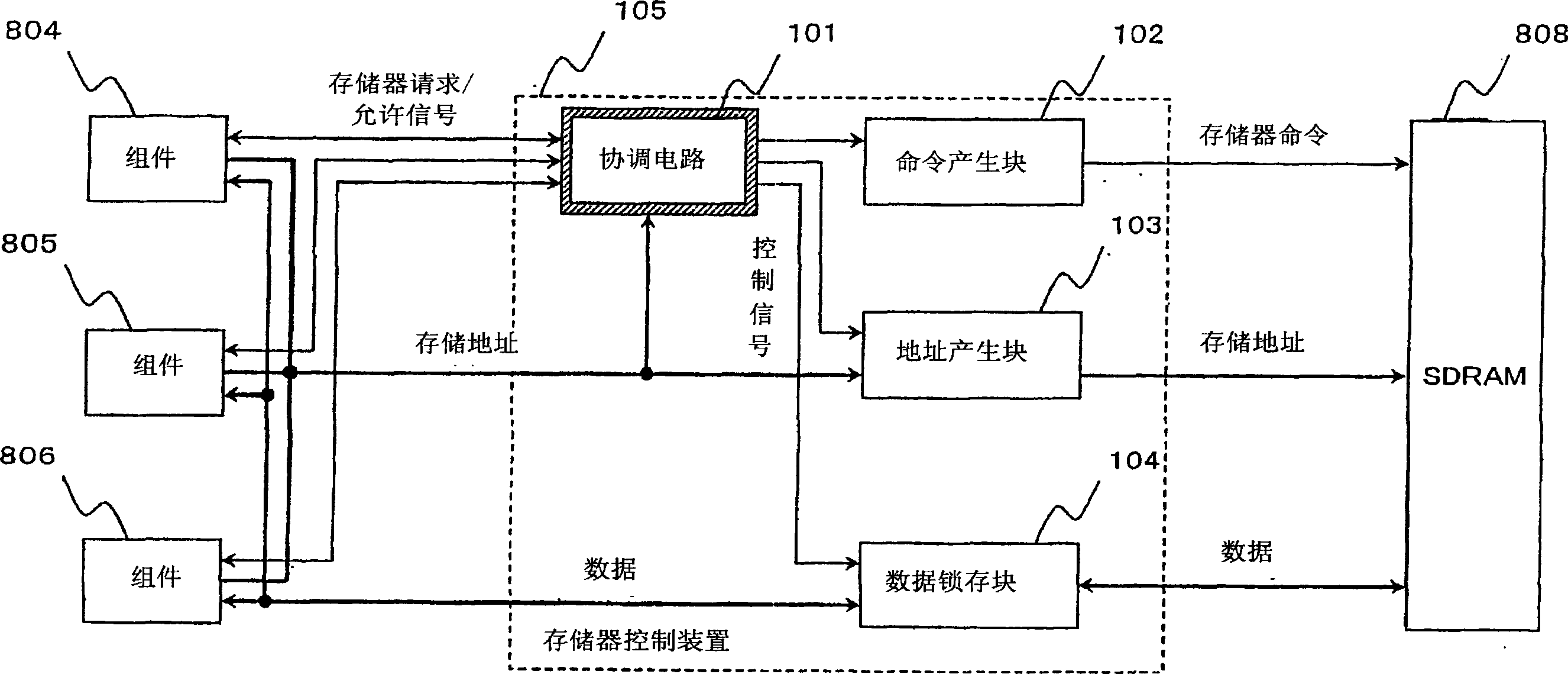
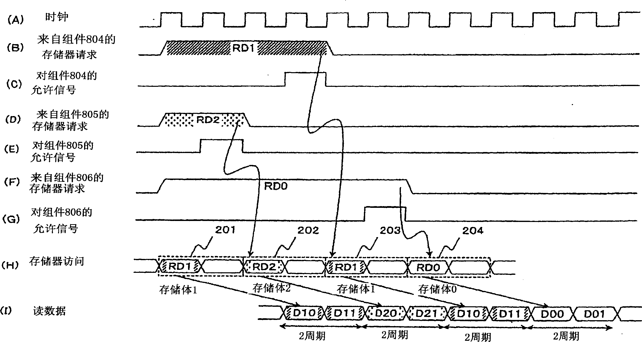
[0085] Below, use figure 1 , figure 2 , Figure 8 and Figure 9 Embodiments of the first to eighth inventions will be described. Figure 4 A block diagram showing a memory control device according to Embodiment 1, figure 2 yes figure 1 8 is a block diagram showing the coordination circuit of the first embodiment.

[0086] Such as figure 1 As shown, the components of the memory control device 105 include a coordinating circuit 101 for coordinating the memory access requests sent by a plurality of components 804, 805, and 806 for accessing the SDRAM 808, a command generation block 102 for generating memory commands to the SDRAM 808, and a receiving The storage address sent by the components that the coordination circuit 101 allows access is output to the address generation block 103 of the SDRAM808, and the write data sent by the components that the coordination circuit 101 allows access or from the SDRAM808 The read data is latched, and a data latch block 104 that all...

Embodiment approach 2

[0151] Below, use figure 1 , image 3 , Figure 10 and Figure 11 Embodiments of the ninth to fourteenth present inventions will be described. image 3 is the main signal timing diagram of Embodiment 2, Figure 10 is a block diagram showing the coordination circuit 101 according to Embodiment 2, Figure 11 It is a block diagram showing the data latch block 104 of the second embodiment.

[0152] Regarding the composition of the memory control device 105, because it is the same as that of Embodiment 1 ( figure 1 ) are the same, so that the reference numbers in the figures are the same, and the description is omitted.

[0153] Such as figure 1 , Figure 10 As shown, the components of the coordinating circuit 101 include receiving memory requests and storage addresses from the multiple components 804, 805, 806 and judging the second half of the storage banks that allow memory access at present according to the received storage addresses and Whether the first half memor...

Embodiment approach 3

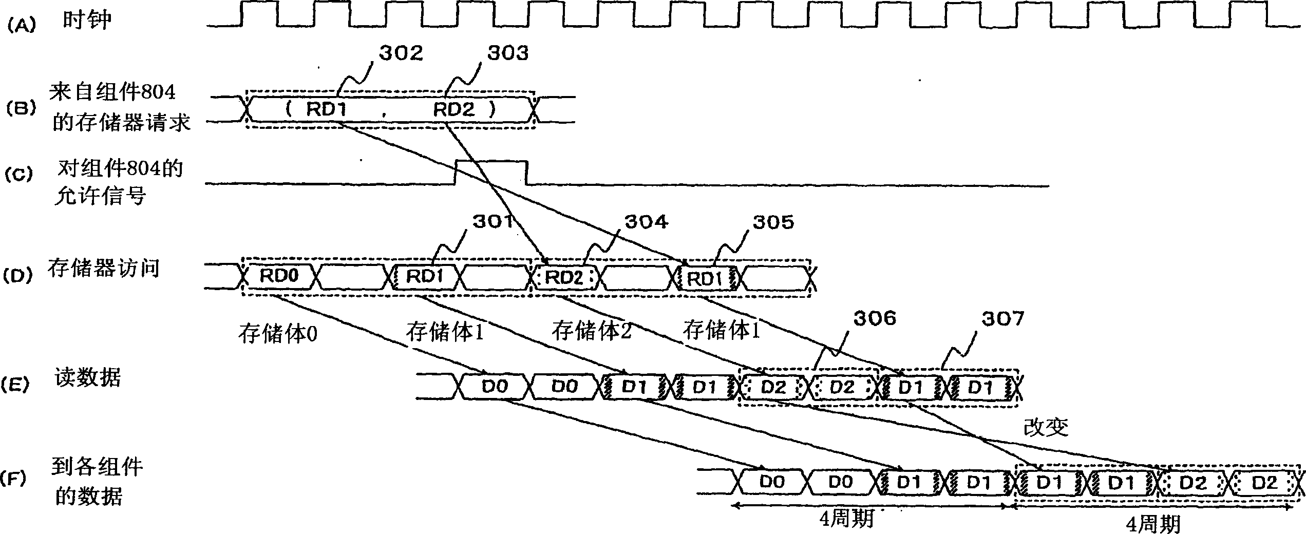
[0185] Below, use figure 1 , Figure 4 and Figure 12 Embodiments of the fifteenth to nineteenth inventions will be described. Figure 4 is the main signal timing diagram of Embodiment 3, Figure 12 It is a block diagram showing the cooperation circuit of Embodiment 3.

[0186] Regarding the composition of the memory control device 105, because it is the same as that of Embodiment 1 ( figure 1 ) are the same, so that the reference numbers in the figures are the same, and the description is omitted.

[0187] Such as figure 1 , Figure 12 As shown, the components of the coordinating circuit 101 include a data unit judging unit 1402 that receives memory requests from the plurality of components 804, 805, and 806 and judges the data units of the requested memory access according to the received memory requests and A request receiving block 1401 that instructs generation of a permission signal, a memory access priority specifying unit 1003 that specifies the priority of m...


PUM


Abstract

There is provided a memory control device which prevents continuous access to the same bank of an SDRAM, thereby improving the processing time. The memory control device (105) controls a memory including a plurality of banks which can be accessed continuously by the bank division mode. The priority of the blocks (804, 805, 806) accessing the SDRAM (808) via the memory control device (105) is controlled in such a manner that memory access requests from these blocks continuously access different banks of the SDRAM (808).

Description

field of invention [0001] The present invention relates to a memory control device for controlling a memory composed of a plurality of memory banks in electronic equipment. Background technique [0002] In recent years, a synchronous dynamic random access memory (hereinafter abbreviated as SDRAM) capable of high-speed burst transfer of a cache memory frequently used in personal computers in synchronization with a clock has been used. This SDRAM can switch the sequential access mode and the random access mode of the bank division mode. In the bank division mode, as four memory areas, there are: bank 0 whose 2-bit bank signal is "00", bank 1 which is "01", bank 2 which is "10", and which is "11" storage bank 3. While switching the memory bank 0, memory bank 1, memory bank 2, and memory bank 3 by clock control, access is performed, and the address of the next memory bank can be set during the period when data is read from the first accessed memory bank. take in. [0003] Su...

Claims


Application Information

Patent Timeline
Patent Type & Authority Applications(China)
IPC IPC(8): G06F12/06G06F12/00G06F13/16
CPCG06F12/0607G06F13/161G06F13/1647G06F12/00
Inventor 秋月麻水子青木透上田泰志
Owner PANASONIC CORP
Why Eureka
Try Eureka