Electroluminescent device of organic thin film

An electroluminescent device and organic thin film technology, applied in the field of organic thin film electroluminescent devices, can solve the problems of interdiffusion, insufficient balance between holes and electrons, and inability to prepare high-performance organic light-emitting devices, so as to improve interdiffusion, efficiency and performance. Life-enhancing effect

Inactive Publication Date: 2006-02-01
BEIJING JIAOTONG UNIV
View PDF0 Cites 9 Cited by
  • Summary
  • Abstract
  • Description
  • Claims
  • Application Information

AI Technical Summary

Problems solved by technology

However, in order to obtain high-brightness, high-efficiency and long-life organic electroluminescent devices, some problems in organic electroluminescence have not been well resolved, such as the limitations of current hole and electron transport layer materials and preparation processes. , with the structure of ordinary organic electroluminescent devices: ITO / hole transport layer / organic light-emitting layer / back electrode, there are some problems as follows: mutual diffusion between the light-emitting layer and the electrode, not enough hole and electron mobility , and the injected holes and electrons are not balanced enough, etc.
These problems limit the further improvement of organic electroluminescent devices and become an important bottleneck in the development of organic electroluminescent devices, making it impossible to prepare organic light-emitting devices with excellent performance.

Method used


Image

  • Electroluminescent device of organic thin film

Examples


Embodiment Construction

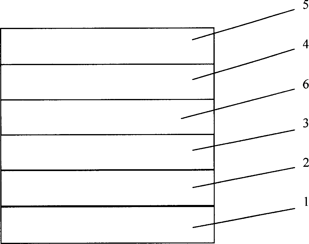
[0010] The present invention will be further described by taking the accompanying drawings as embodiments. The novel electron transport layer organic thin film electroluminescent device is composed of a hole transport layer 2, an organic light-emitting layer 3, an inorganic electron transport layer 6, an electron potential compensation layer 4 and a back electrode 5 sequentially prepared on a transparent electrode 1.

[0011] The electron potential compensation layer 4 is made of lithium fluoride LiF, located between the electron transport layer 6 and the back electrode 5, and the thickness of the electron potential compensation layer 4 is 0.2nm-0.6nm. When the energy of the back electrode 5 and the electron transport layer 6 are matched, the electron potential compensation layer 4 is canceled.

[0012] The inorganic electron transport layer 6 is made of n-type zinc sulfide ZnS, which is located between the light-emitting layer 3 and the electron potential compensation layer 4...


PUM


Abstract

The Electroluminescent device is composed of following layers and parts prepared on clear electrode: cavity transport layer, organic luminous layer, inorganic electron transport layer, electronic potentiometric compensator layer and back electrode. Inorganic electron transport layer is prepared from n type ZnS or n type ZnO with thickness 1nm-10nm. Inorganic electron transport layer is also prepared from other n type wide forbidden band inorganic materials: n type CoO, n type GaN, n type BaO, n type MgO or n type AIN. The invention raises luminescence brightness, efficiency and service life since mutual diffusion between luminous layer and electrode in electroluminescent device and inadequate balance between cavities and electrons are improved in the disclosed structure.

Description

technical field [0001] The invention relates to an organic thin film electroluminescent device, which is mainly used for producing an organic thin film electroluminescent device with high brightness, efficiency and long life. Background technique [0002] Since Deng Qingyun C.W.Tang of Kodak Company of the United States reported organic electroluminescence in 1987, there has been an upsurge in the research of organic thin film light-emitting diodes all over the world. Organic thin-film light-emitting diodes have unique advantages such as active light emission, fast response, full solidification, easy colorization, and low driving voltage. They are very potential flat panel displays that will replace the current liquid crystal displays that dominate the market. It is precisely because of its background in the field of flat panel display that many companies, universities and research institutes have invested a lot of manpower and material resources in organic electroluminescen...

Claims


Application Information

Patent Timeline
Patent Type & Authority Applications(China)
IPC IPC(8): H05B33/20H05B33/12
Inventor 张希清姚志刚杜鹏
Owner BEIJING JIAOTONG UNIV
Why Eureka
Try Eureka