Print circuit board with improved heat rejection structure and electronic device

A technology of printed circuit board and heat dissipation structure, which is applied in the direction of printed circuit and circuit where printed circuit components and non-printed electrical components are connected, and can solve the problems of inability to provide heat dissipation effect, high heat dissipation rate, and inability to dissipate heat.

Active Publication Date: 2006-02-08
VIA TECH INC
View PDF0 Cites 7 Cited by
  • Summary
  • Abstract
  • Description
  • Claims
  • Application Information

AI Technical Summary

Problems solved by technology

[0005] However, for high-power chips that generate high heat, the above-mentioned passive cooling cannot provide optimal heat dissipation effect and high heat dissipation rate.
That is t

Method used


Image

  • Print circuit board with improved heat rejection structure and electronic device
  • Print circuit board with improved heat rejection structure and electronic device
  • Print circuit board with improved heat rejection structure and electronic device

Examples


Embodiment Construction

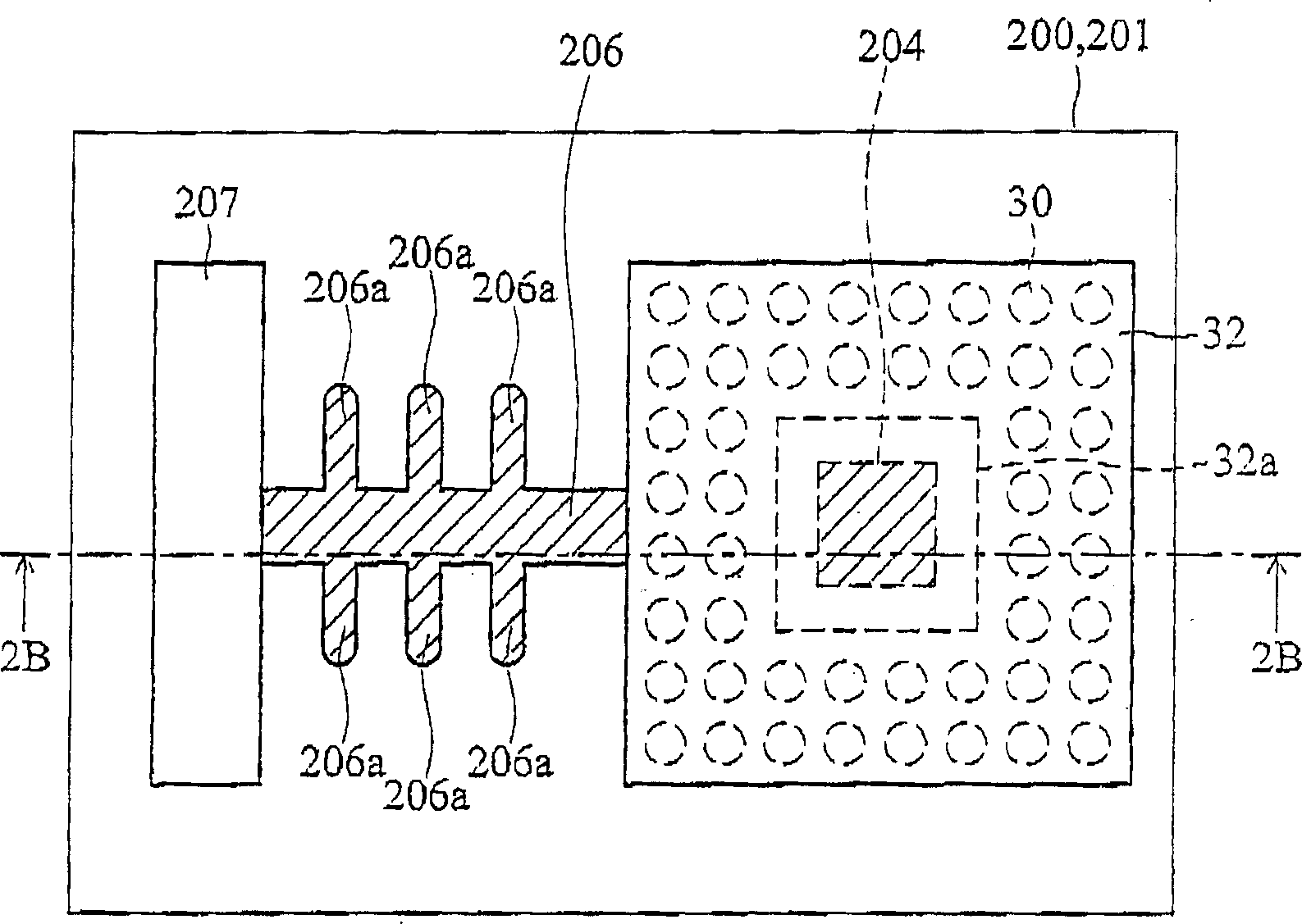
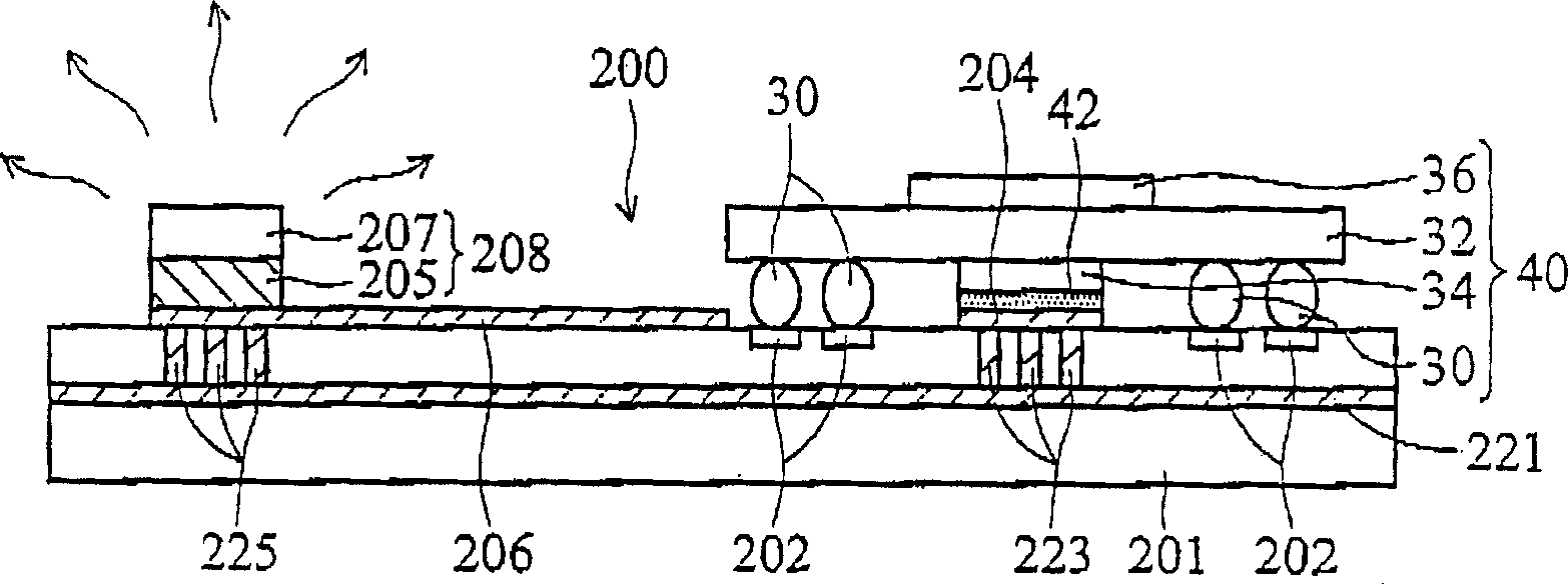
[0027] The following fit Figure 2A and Figure 2B An electronic device with an improved heat dissipation structure is described according to an embodiment of the present invention, wherein Figure 2A shows a schematic plan view of an electronic device with an improved heat dissipation structure according to an embodiment of the present invention, and Figure 2B showing along Figure 2A Schematic cross-sectional view of line 2B-2B. The electronic device includes: a multi-package module 40 , a circuit board 200 , a heat conduction layer 204 and a heat sink 206 .

[0028] The multi-package module 40 includes a package substrate 32 . The lower surface of the package substrate 32 has a chip area 32 a and the upper surface also has a chip area (not shown). Here, "lower surface" refers to the surface facing the circuit board (eg, printed circuit board), and "upper surface" refers to the surface facing away from the lower surface. In this embodiment, the package substrate 32 ca...


PUM


Abstract

This invention discloses a printed circuit board to improve dissipating heat structure, suitable for a packing base plate of multiply packing blocks, which comprises a first top layer located on a base plate and relative to a pack base plate, a second top metal layer located on the base plate and on the side of pack base plate; a inner metal layer located in the base plate; a first and second heat conducting bullet located in the base to make the inner metal layer individually linked to the first top layer and the second one. The invention also discloses a electron device to better dissipating structure.

Description

Technical field: [0001] The present invention relates to an electronic device, in particular to an electronic device with an improved heat dissipation structure and a multi-package module (MPM). Background technique: [0002] Portable electronic products, such as cell phones, mobile computing and other consumer products need to exhibit high performance and functionality under the constraints of thin thickness, light weight and low cost. Therefore, manufacturers are driven to increase the density of semiconductor chips. That is, manufacturers have begun to turn to three-dimensional (3D) packaging, and multiple chips are stacked in one package by assembly techniques such as wire bonding or flip chip. [0003] Therefore, multi-package module (multi-package module, MPM) has recently attracted more and more attention, which can integrate chips with different functions on a package substrate, such as microprocessors or memory, logic and optical integrated circuits, etc., replacin...

Claims


Application Information

Patent Timeline
IPC IPC(8): H05K1/18H05K7/20H05K1/02H01L27/00H01L23/36
CPCH01L2924/0002
Inventor 林志雄张乃舜
Owner VIA TECH INC
Why Eureka
Try Eureka