Semiconductor optical amplifier
A technology of optical amplifiers and semiconductors, applied in the directions of instruments, optics, nonlinear optics, etc., can solve the problems of difficult process, inconvenient application, complex structure, etc., and achieve the effect of high degree of particle number inversion, easy realization, and simple structure
- Summary
- Abstract
- Description
- Claims
- Application Information
AI Technical Summary
Problems solved by technology
Method used
Image
Examples
Embodiment Construction
[0020] The present invention will be further described below in conjunction with the embodiments and accompanying drawings.
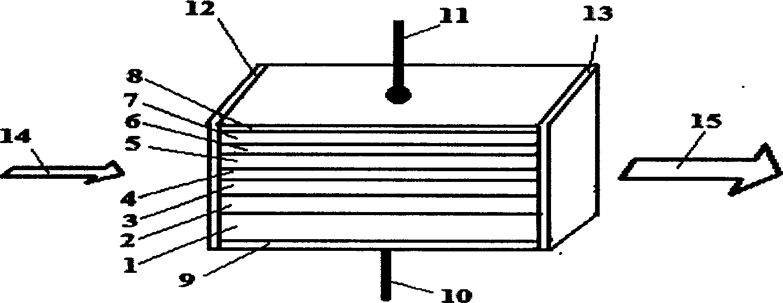
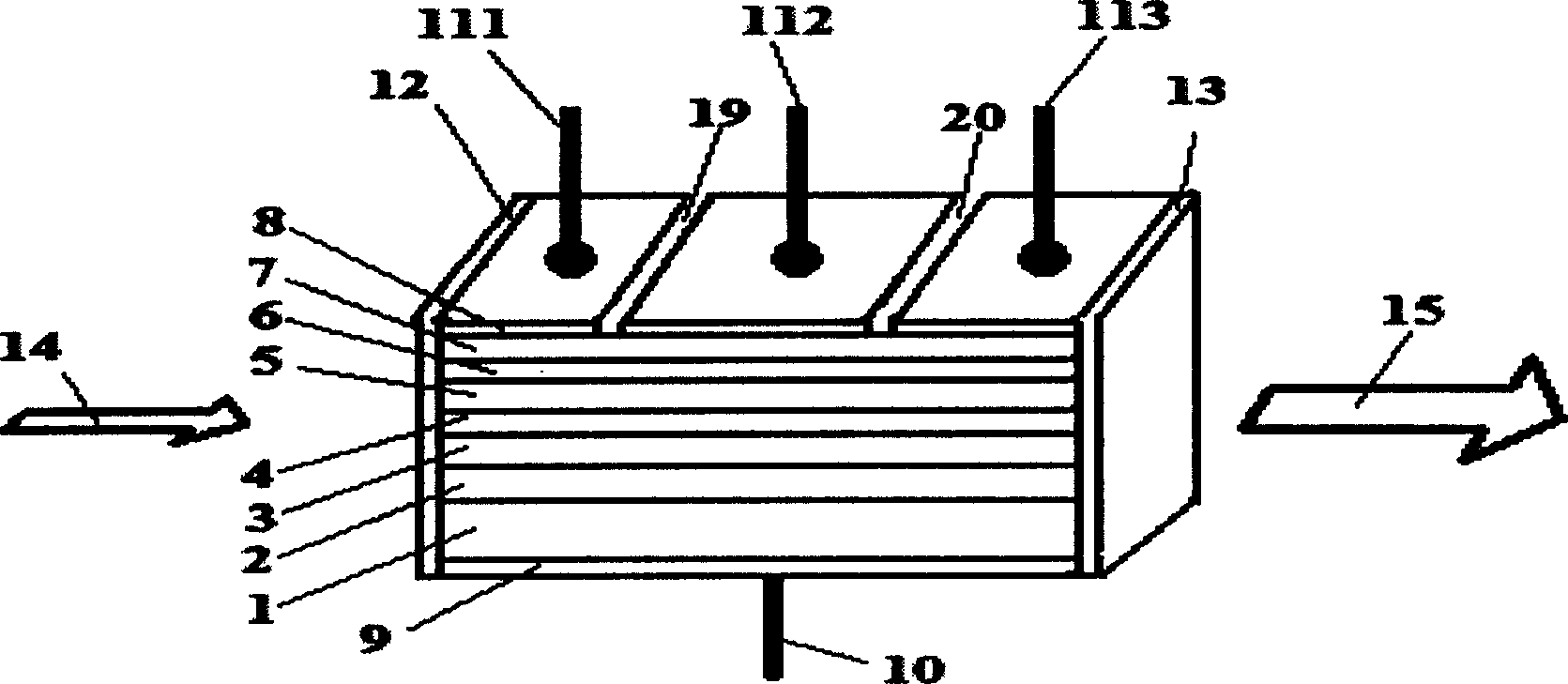
[0021] image 3 It is a structural schematic diagram of an embodiment of the present invention. The SOA shown is a typical structure in which quantum wells are used as the active region. Its interior consists of a substrate 1, a buffer layer and a lower cladding layer 2, a lower confinement layer 3, an active region 4, an upper confinement layer 5, and an upper cladding layer. 6. The ohmic contact layer 7 is formed sequentially. An anti-reflection film 12 and an anti-reflection film 13 are plated on the input end face and output end face of the amplifier. The top layer and the bottom layer of the amplifier are the upper metal electrode layer 8 and the lower metal electrode layer 9 respectively; the lower electrode 10 is made under the lower metal electrode layer 9 . The input signal light 14 enters the interior of the SOA, and it can be continuously ...
PUM
 Abstract
Description
Claims
Application Information


