Photolithography device and method for manufacturing the same

A lithography and accommodating device technology, applied in microlithography exposure equipment, photolithographic process exposure devices, patterned surface photolithographic process, etc. Imaging effect

Inactive Publication Date: 2006-02-15
INFINEON TECH AG
View PDF3 Cites 3 Cited by
  • Summary
  • Abstract
  • Description
  • Claims
  • Application Information

AI Technical Summary

Problems solved by technology

[0008] These effects in known lithographic setups, especially at small structure sizes, lead to quality problems in t

Method used


Image

  • Photolithography device and method for manufacturing the same
  • Photolithography device and method for manufacturing the same
  • Photolithography device and method for manufacturing the same

Examples


Embodiment Construction

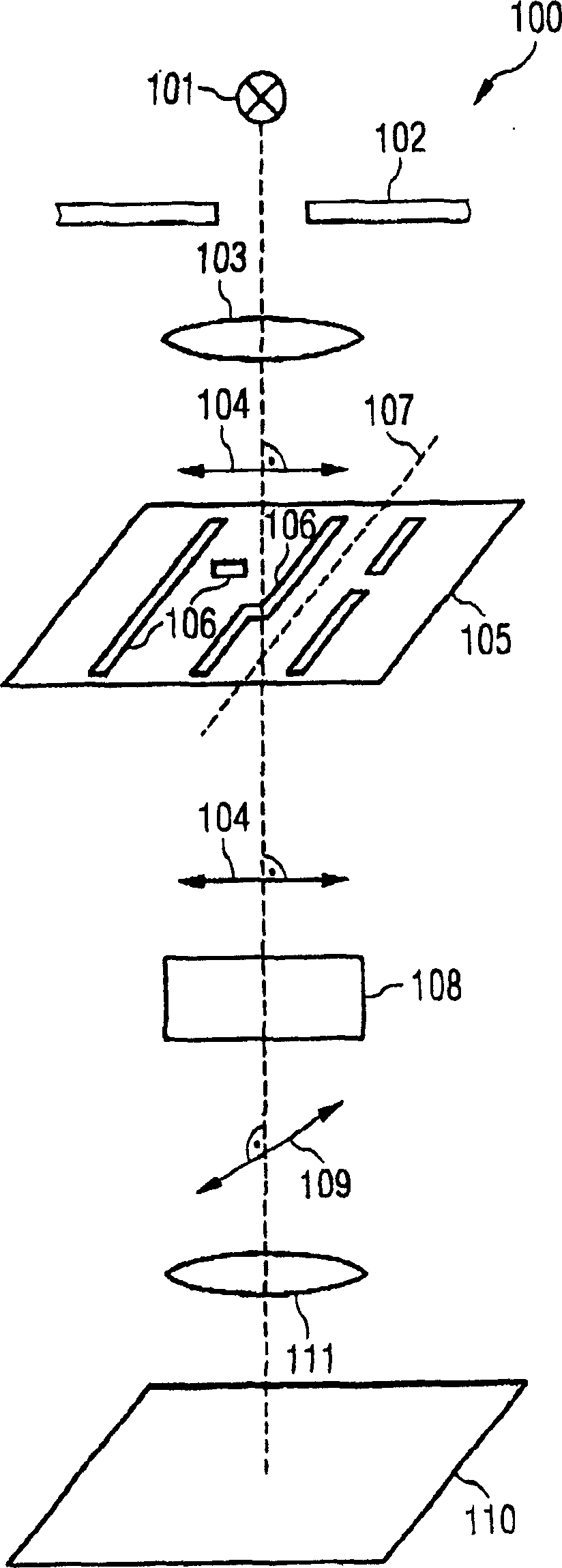
[0056] Next, with figure 1 And a photolithographic apparatus 100 is described according to a preferred embodiment of the present invention.

[0057] figure 1 The illustrated lithographic apparatus 100 comprises an electromagnetic radiation source 101, for example an ArF radiation source, which emits electromagnetic radiation with a wavelength of 193 nm. The light system emitted from the electromagnetic radiation source 101 is linearly polarized and has a polarization vector 104 . The generated electromagnetic radiation is directed through an aperture 102 and a lens 103 onto a mask 105 .

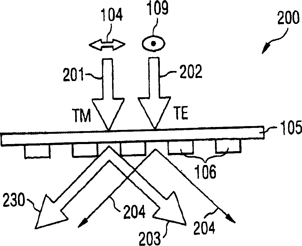
[0058] The photomask 105 includes a plurality of structures 106 to be formed on a silicon wafer 110 . The structure 106 comprises different components, which are generally arranged along an extension direction 107 . Electromagnetic radiation is absorbed by structures 106 and passes through regions between structures 106 . The first polarization vector 104 is substantially perpendicular t...


PUM


Abstract

A photolithography device includes a photomask having multiple structures, the isostructural system extends along the presupposed and the course direction of the photomask; a mean for generating an electromagnetic radiation and introducing the electromagnetic radiation to the photomask, the electromagnetic radiation is at least partially TM-polarized relative to the course direction, so that the TM-polarized electromagnetic radiation has a polarization direction at an angle of 90 DEG with respect to the course direction; a receptacle device for receiving a substrate to be exposed is positioned so that the radiation impinges on the substrate.

Description

technical field [0001] The present invention relates to a photolithography device and a method for manufacturing the photolithography device. Background technique [0002] Photolithography is a printing-on-replication method in which a pattern is imprinted on a material by means of light exposure. Photolithography technology is very important in printing technology and semiconductor technology. [0003] In semiconductor technology, the structural information of a mask can be transferred to the photoresist on a semiconductor substrate (eg, a silicon wafer) by means of photolithography. After development of the hidden image, the structural information can be transferred to the semiconductor substrate below the photoresist by means of etching, after which the photoresist layer is removed. [0004] The repetition of this process, with different successive layers and the fine adjustment of a single pattern, is a key technique in the manufacture of integrated circuits (so-called...

Claims


Application Information

Patent Timeline
IPC IPC(8): G03F7/20G03F7/00H01L21/027
CPCG03F7/70566
Inventor M・尼伊霍夫
Owner INFINEON TECH AG
Why Eureka
Try Eureka