Method for producing resist substrates
A technology of resist layer and negative resist, applied in photosensitive materials for opto-mechanical equipment, hologram writing methods, record carriers used by machines, etc., can solve problems such as time-consuming and increasing processing time. , to achieve the effect of large beam width, reduced exposure time and increased effective exposure dose
- Summary
- Abstract
- Description
- Claims
- Application Information
AI Technical Summary
Problems solved by technology
Method used
Image
Examples
Embodiment Construction
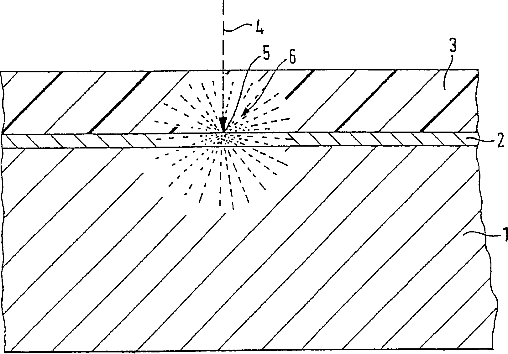
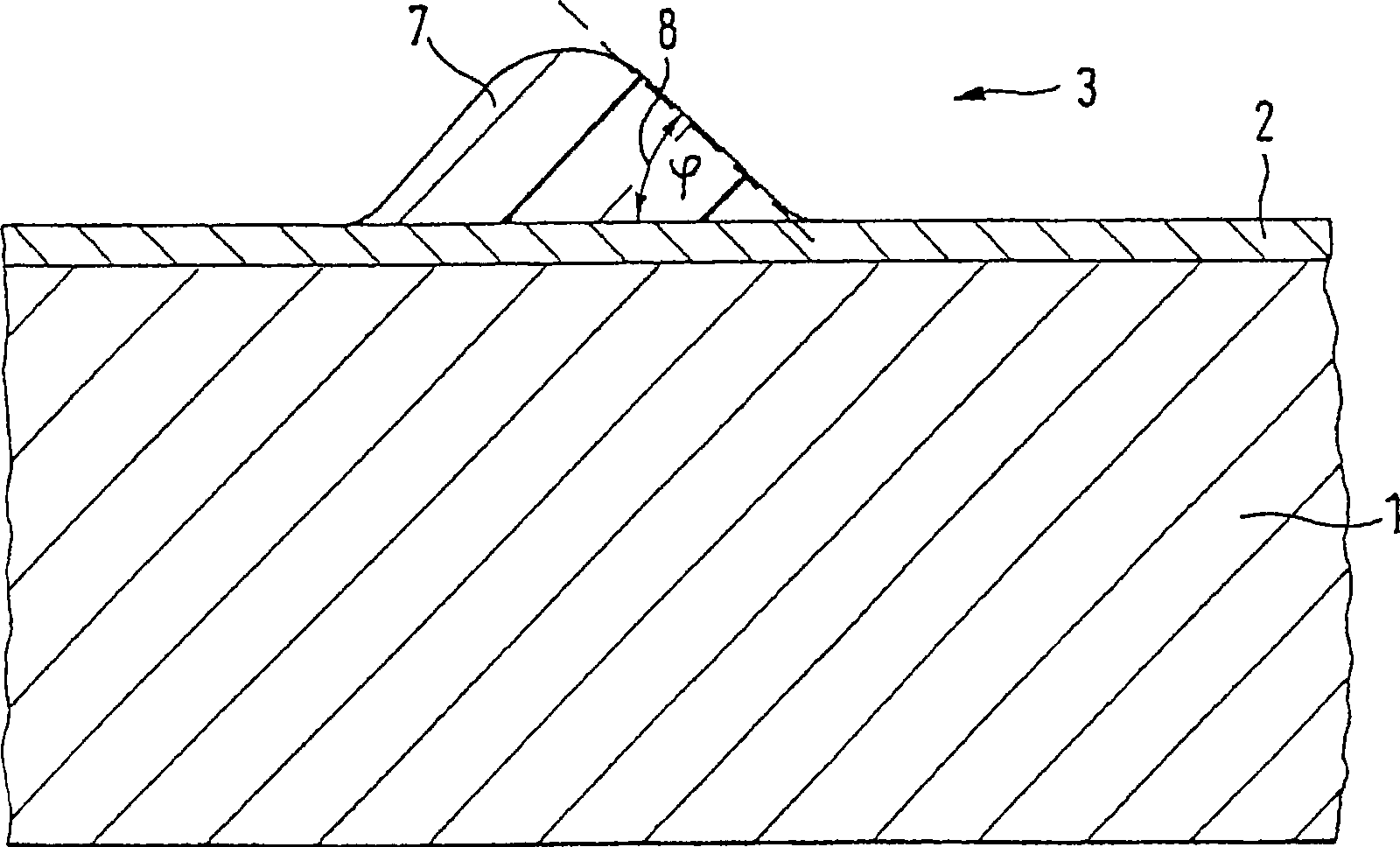
[0041] Figure 1A is a cross-sectional view of a substrate 1 on which a conductive layer 2 made of a conductive material is coated. The conductive layer 2 can be produced, for example, from metals, metal alloys or conductive polymers. On the conductive layer 2 is located a resist layer 3 made of a negative resist. Since the negative resist 3 is generally non-conductive, the conductive layer 2 serves to redirect the electrons incident with the electron beam 4 . When the substrate 1 is sufficiently conductive, the conductive layer 2 can be discarded.
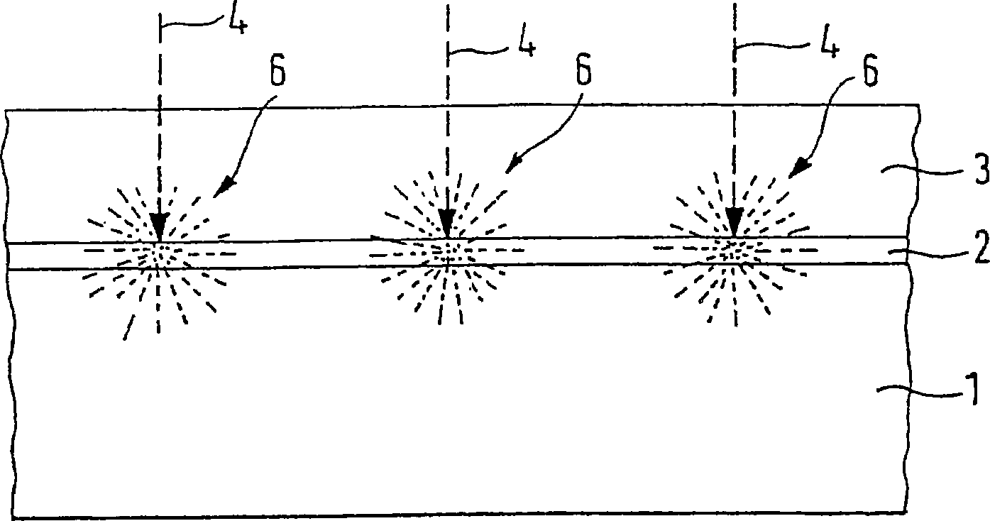
[0042] Since the conductive layer 2 scatters the primary electrons incident with the electron beam 4 and additionally emits secondary electrons by the conductive layer 2, an exposure region 6 is formed near the target region 5 hit by the electron beam 4, through which the adjacent target region 5 Areas of negative resist 3 are exposed. The range of the exposure area 6 is determined by the material used, the electron acceleratio...
PUM
 Abstract
Description
Claims
Application Information


