Method for producing resist substrates

A technology of resist and resist layer, which is applied in the field of preparing substrates, can solve the problems of time-consuming and increased processing time, and achieve the effects of large beam width, reduced exposure time, and excellent separation performance

Inactive Publication Date: 2006-03-29
GIESECKE & DEVRIENT GMBH
View PDF0 Cites 1 Cited by
  • Summary
  • Abstract
  • Description
  • Claims
  • Application Information

AI Technical Summary

Problems solved by technology

[0014] These known methods are time consuming and require special types of resists that are tuned for side issues and are not optimal for their other properties
The multiple exposure process used to form the sides and working with different types of resists adds significantly to the processing time

Method used


Image

  • Method for producing resist substrates
  • Method for producing resist substrates
  • Method for producing resist substrates

Examples


Embodiment Construction

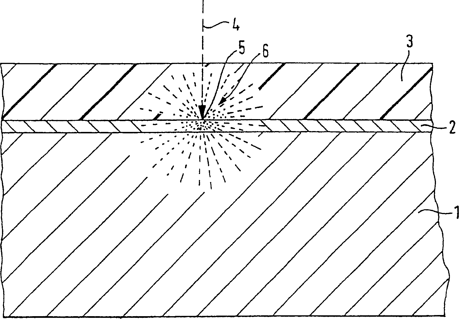
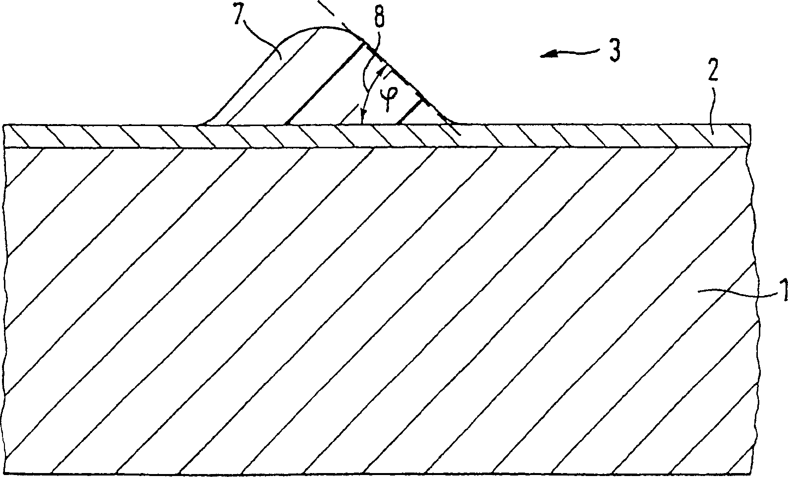
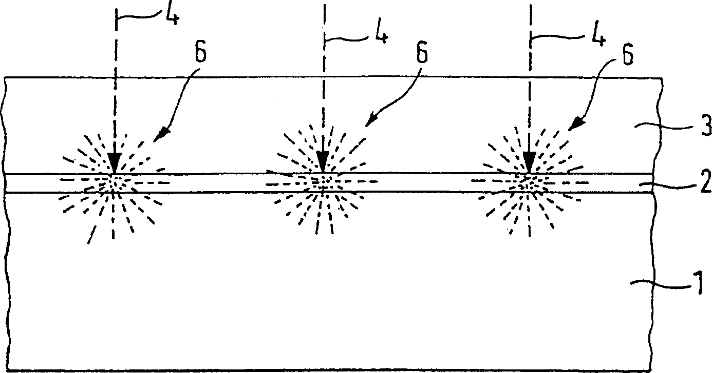
[0041] Figure 1A is a cross-sectional view of a substrate 1 on which a conductive layer 2 made of a conductive material is coated. The conductive layer 2 can be produced, for example, from metals, metal alloys or conductive polymers. On the conductive layer 2 is located a resist layer 3 made of a negative resist. Since the negative resist 3 is generally non-conductive, the conductive layer 2 serves to redirect the electrons incident with the electron beam 4 . When the substrate 1 is sufficiently conductive, the conductive layer 2 can be discarded.

[0042] Since the conductive layer 2 scatters the primary electrons incident with the electron beam 4 and additionally emits secondary electrons by the conductive layer 2, an exposure region 6 is formed near the target region 5 hit by the electron beam 4, through which the adjacent target region 5 Areas of negative resist 3 are exposed. The range of the exposure area 6 is determined by the material used, the electron acceleratio...


PUM


Abstract

The invention relates to a method for producing a substrate provided with a resist layer in the form of a relief structure comprising a diffraction structure. Said resist layer interacts with at least areas provided with a conductive layer which diffuses primary electrons and / or produces secondary electrons when the resist layer is exposed to an electron beam effect. For the inventive method, the material of the resist and conductive layers and exposition parameters are co-ordinated therebetween in such a way that the resist layer is also exposed outside the area exposed to the electron beam in such a way that the lateral parts of the relief structure hold an inclined shape.

Description

technical field [0001] The present invention relates to a method for preparing a substrate having a resist layer in the form of a relief structure representing a diffractive structure and having a conductive layer formed on the resist layer by an electron beam Scatter primary electrons and / or generate secondary electrons upon exposure. [0002] Furthermore, the present invention relates to resist masters and resist substrates. Background technique [0003] Optically variable elements whose optical properties vary with viewing angle are frequently used not only for preventing counterfeiting or copying of value documents such as credit cards, banknotes, but also for product protection of any product packaging. These optically variable elements have diffractive structures of true holograms, computer holograms, or grating images with grating fields placed side by side. Generally speaking, a hologram is a superposition of diffraction gratings. However, grating images are const...

Claims


Application Information

Patent Timeline
Patent Type & Authority Applications(China)
IPC IPC(8): G03F7/09H01J37/317G03F7/00G03F7/20G02B5/18G06K19/16
CPCG06K19/16G02B5/1857G03F7/0005G03F7/09G03F7/2059G03F7/2061G03H1/0244G03H1/0891G03H2001/0478G03H2224/04G03H2260/14G03H2260/63Y10S430/143
Inventor 威蒂克·考尔
Owner GIESECKE & DEVRIENT GMBH
Why Eureka
Try Eureka