Eureka AIR delivers breakthrough ideas for toughest innovation challenges, trusted by R&D personnel around the world.

Electronic circuit packaging process

A packaging process and electronic circuit technology, applied in the direction of circuits, electrical components to assemble printed circuits, electrical components, etc., can solve the problems of low efficiency and difficult packaging, and achieve the effect of reducing the size of the device

Inactive Publication Date: 2006-04-26
上海三基电子工业有限公司
View PDF0 Cites 3 Cited by
  • Summary
  • Abstract
  • Description
  • Claims
  • Application Information

AI Technical Summary

Problems solved by technology

[0004] However, for electronic component arrays or combined circuits, the above-mentioned packaging process is inefficient and difficult to package qualified products.

Method used


Image

  • Electronic circuit packaging process
  • Electronic circuit packaging process
  • Electronic circuit packaging process

Examples


Embodiment Construction

[0014] The encapsulation process of the present invention will be further described below with reference to the drawings and embodiments.

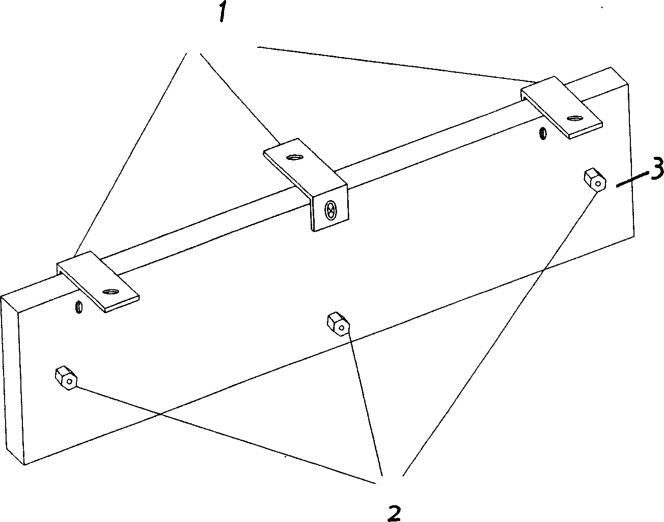
[0015] refer to figure 1 , which is a schematic diagram of the printed board electronic component assembly board of the present invention.

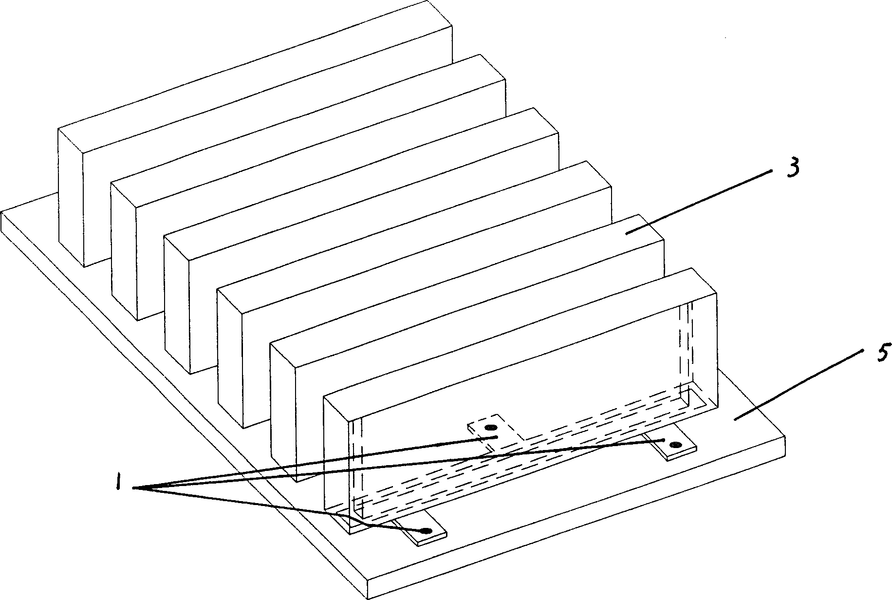
[0016] As shown in the figure, 1 is the supporting foot, which is used to fix the printed board cover assembly and install it on the large printing plate (base), 2 is the positioning column, which is used to fix the spacing between multiple printed board cover components, and 3 is Printed board coats electronic components.

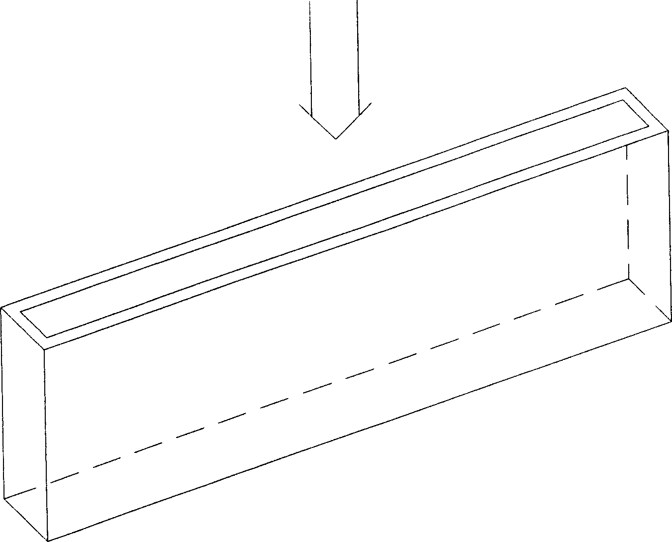
[0017] refer to figure 2 , which is a schematic diagram of a metal or non-metal box for a printed board electronic component assembly board of the present invention.

[0018] As shown in the figure, this is a rectangular box made of metal with an opening on one side for placing the printed sleeve assembly. The metal material is used for shielding and the effect is good. Non-m...


PUM


Abstract

The invention relates to package technology for electronic circuit, which comprises: first, preparing electronic component array or discrete circuit of combined circuit with electrical characteristics output by location frame; second, laying a metal sheath or nonmetal case to the discrete circuit; third, pouring epoxy resin inside shell to package; fourth, drying the resin, inverting the poured component to fix on large print board by screw and supporting hole; finally, fixing a plurality of discrete modules on substrate to form a circuit integer by interconnection with wire. This invention cuts device volume, improves reliability, and has some economical benefit.

Description

technical field [0001] The invention relates to a packaging process for electronic circuits, more specifically to a packaging process for arrays of electronic components or combined circuits, and belongs to the technical field of electronic packaging. Background technique [0002] For arrays or combined circuits of various electronic components, in order to consider confidentiality and easy installation and maintenance, the modules can be packaged in metal or non-metallic casings to improve the electromagnetic compatibility characteristics of products and improve the reliability of electronic components or combined circuits. Confidentiality and market competitiveness. [0003] For current electronic components, only in the case of confidentiality, a certain or a group of components is simply placed in a special metal or non-metal box, and the inside is filled with epoxy resin to encapsulate it. This is a relatively common and commonly used process method. [0004] However,...

Claims


Application Information

Patent Timeline
IPC IPC(8): H01L21/50H01L23/02H01L25/00H05K3/30
Inventor 陈银华王丽萍
Owner 上海三基电子工业有限公司
Why Eureka
Eureka Blog
Learn More