Optical member,optical connector and electronic parts and instrument

A technology for optical devices and electronic devices, which is applied in the direction of printed circuits, electrical solid devices, and semiconductor devices connected with non-printed electrical components. It can solve problems such as non-transfer molding technology and achieve the effect of reducing costs.

Inactive Publication Date: 2006-04-26
SHARP KK
View PDF3 Cites 8 Cited by
  • Summary
  • Abstract
  • Description
  • Claims
  • Application Information

AI Technical Summary

Problems solved by technology

[0009] However, the resin molded body of the above-mentioned conventional electronic device is made by sandwiching the flexible substrate mounted with the optical sensor with the injection mold, pressurizing it, and filling it with thermoplastic resin, which is not suitable for transfer molding technology.

Method used


Image

  • Optical member,optical connector and electronic parts and instrument
  • Optical member,optical connector and electronic parts and instrument
  • Optical member,optical connector and electronic parts and instrument

Examples


no. 1 Embodiment approach

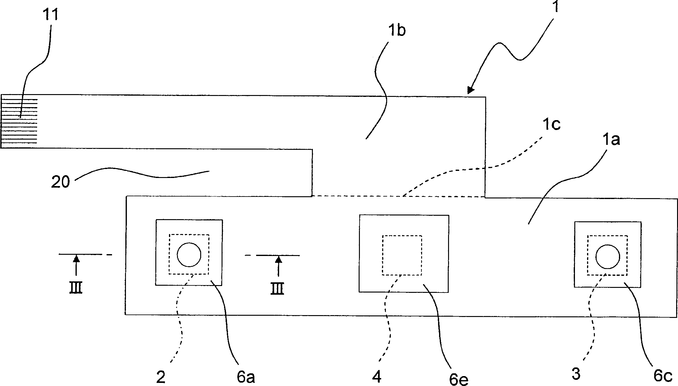
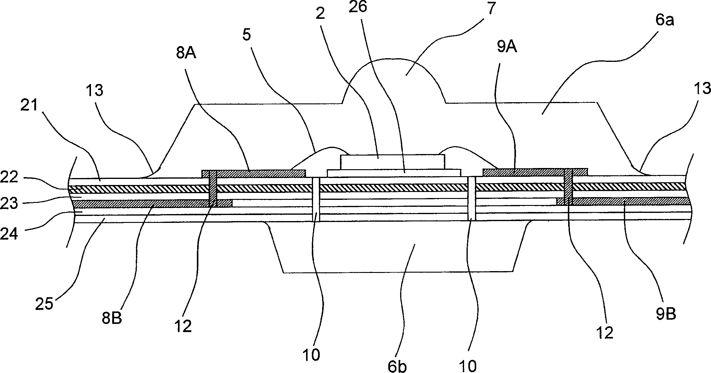
[0070] figure 1 It is a plan view of an optical device which is an example of the electronic device according to the first embodiment of the present invention, figure 2 From figure 1 Side view of the aforementioned optics seen below. Such as figure 1 As shown, the flexible substrate 1 has: a rectangular body portion 1a; an extension portion 1b extending from the center of the body portion 1a to the side and bent in the longitudinal direction of the body portion 1a. An external connection terminal 11 is provided at the front end of the extension portion 1b of the above-mentioned flexible substrate 1 . In addition, the above-mentioned flexible substrate 1 includes a flexible base substrate 22 (shown in image 3 ), a first wiring pattern (including image 3 electrode parts 8A, 9A), and on the other side of the base substrate 22, a second wiring pattern (including image 3The electrode part 8B, 9B). A part of at least one of the first and second wiring patterns of the flex...

no. 2 Embodiment approach

[0100] Figure 4 It is a cross-sectional view of an optical device which is an example of an electronic component according to a second embodiment of the present invention. The optical device according to the second embodiment has the same configuration as the optical device according to the first embodiment except for a reinforcing material, and the same components use The same symbol, the description is omitted, and the figure 1 , figure 2 .

[0101] Such as Figure 4 As shown, on the outer peripheral parts connected to the flexible substrate 1 of the first and second sealing bodies 6a and 6b of the first and second molded resin parts, a hard resin (for example, polyimide film) is provided. Reinforcement material 14A, 14B. Also, other hard materials such as Dami-like metals can also be used as the reinforcing materials 14A and 14B.

[0102] In the optical device of the above-mentioned second embodiment, the mold clamping pressure applied to the flexible substrate 1 dur...

no. 3 Embodiment approach

[0105] Figure 5 It is a schematic top view of an optical connector using an optical device as an example of an electronic component according to the third embodiment of the present invention. The optical connector of the third embodiment adopts the optical device of the first embodiment, citing figure 1 , figure 2 .

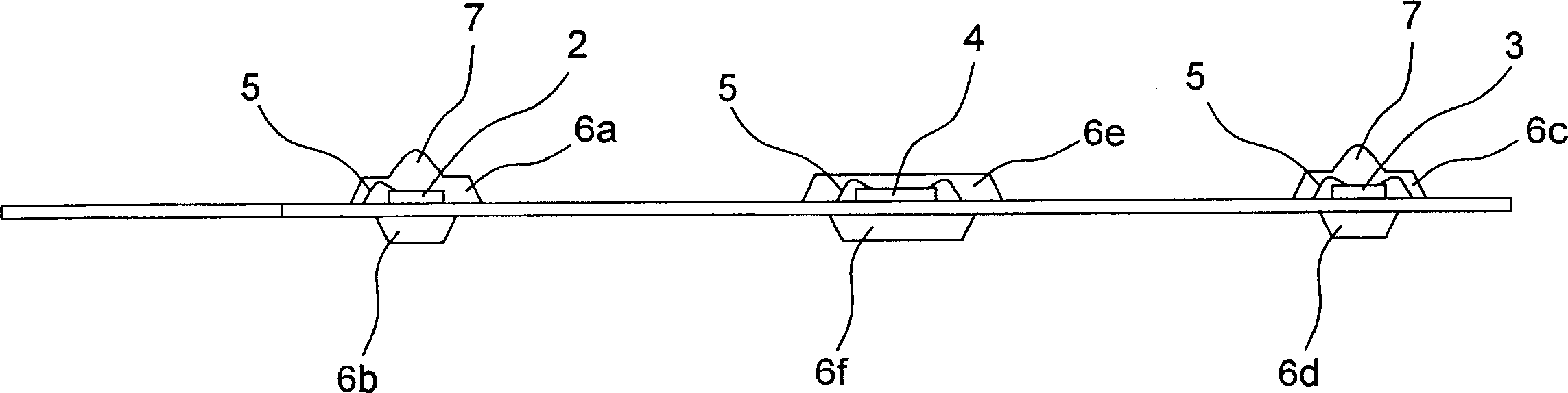
[0106] The optical device of the above-mentioned first embodiment, such as figure 2 As shown, the light-emitting element 2, light-receiving element 3, and communication IC 4 are sealed with independent first sealing bodies 6a, 6c, and 6e by transfer molding, so that leakage of resin to unintended areas can be suppressed. Thus, on the exposed area of ​​the flexible substrate 1, the bypass capacitor 15, the resistive element 16, the crystal oscillator 17, etc., which are examples of the capacitive elements necessary for the light-emitting element 2, the light-receiving element 3, and the communication IC 4, are provided by soldering.

[0107] The optical con...


PUM


Abstract

PROBLEM TO BE SOLVED: To provide an optical device in which the flexibility of arrangement of a light emitting element and a light receiving element is wide and which can deal with various use with high versatility and to provide an optical connector and an electronic apparatus using it.

SOLUTION: The light emitting element 2 and the light receiving element 3 are operated in both sides of the body part 1a of a flexible board 1, and a predetermined interval is opened and carried. The sealing of the translucency is performed for the light emitting element 2 and the light receiving element 3 by the first and second molded resin parts (6a, 6b, 6c and 6d). Thereby, the direction of the position of the light emitting element 2 and the light receiving element 3 and the luminescence side of the light emitting element 2 and the light receiving surface of the light receiving element 3 can be arbitrarily set by utilizing the flexibility of the flexible board 1. The IC 4 for the communication is carried on the flexible board 1 and between the light emitting element 2 and the light receiving element 3, and the IC 4 for the communication is sealed in a third molded resin part (6e, 6f). An extension part 1b extended from the approximate center of the body part 1a of the flexible board 1 and having an external connection terminal 11 is provided at the tip side.

COPYRIGHT: (C)2006,JPO&NCIPI

Description

technical field [0001] The present invention relates to an optical device, an optical connector using the optical device, an electronic device and an electronic device, and is especially suitable for use in electronic devices such as AV (audio-visual) devices and safety devices for home networks and vehicle networks. Background technique [0002] Conventionally, a device in which a light-emitting element and a light-receiving element are mounted on a substrate is regarded as an optical device. The optical device determines the position of the light-emitting element and the light-receiving element and the direction of the light-emitting surface of the light-emitting element and the light-receiving surface of the light-receiving element. Even if the optical connector using this optical device has exactly the same function, the shape of the optical connector varies depending on the application and specification. Therefore, it is necessary to design and produce various optical c...

Claims


Application Information

Patent Timeline
Patent Type & Authority Applications(China)
IPC IPC(8): H01L25/00H05K1/18
CPCH01L2224/48227H01L2924/1815
Inventor 名仓和人
Owner SHARP KK
Why Eureka
Try Eureka