Automatic designing method for ICT test conversion PCB

An automatic design and test point technology, applied in the direction of electronic circuit testing, calculation, measuring device bearings, etc., can solve the problems of low design efficiency, high error rate, manual design, etc., and achieve the effect of improving efficiency and high accuracy

Inactive Publication Date: 2006-06-07
HUAWEI TECH CO LTD
View PDF0 Cites 13 Cited by
  • Summary
  • Abstract
  • Description
  • Claims
  • Application Information

AI Technical Summary

Problems solved by technology

The disadvantage of this design method is that each conversion PCB is manually designed, which makes the design efficiency low; moreover, there are too many manual participation links in the conversion PCB design process, resulting in a high error rate

Method used


Image

  • Automatic designing method for ICT test conversion PCB
  • Automatic designing method for ICT test conversion PCB

Examples


Embodiment Construction
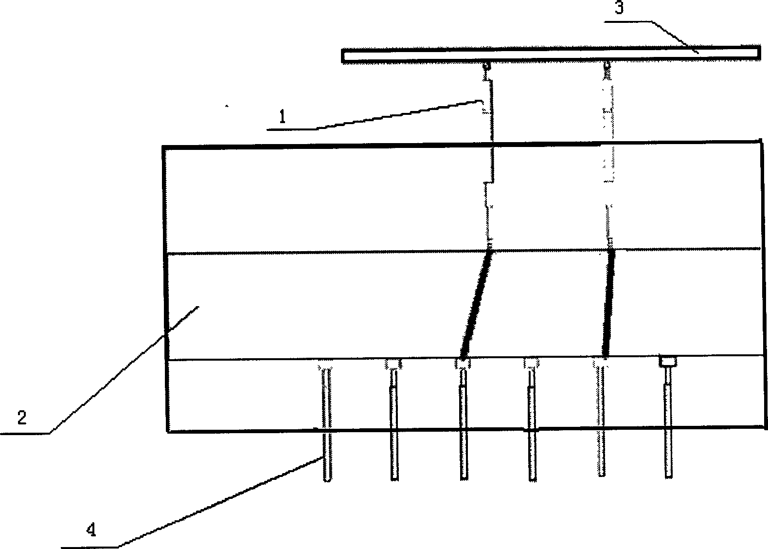
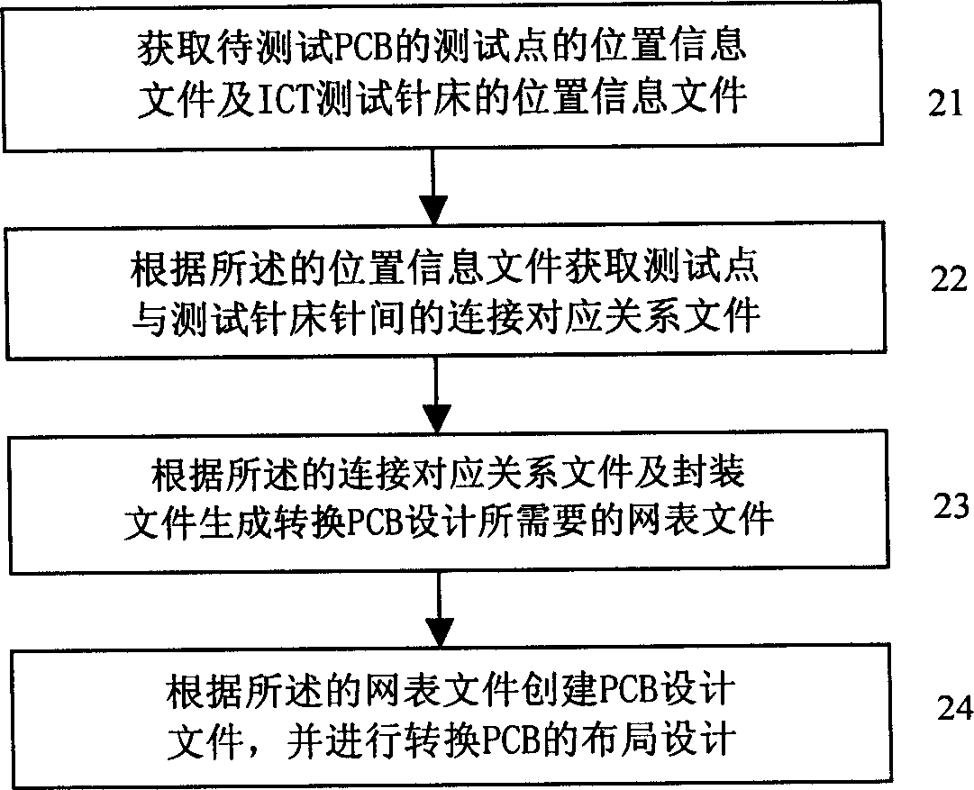
[0043] The core idea of ​​the present invention is to automatically convert the PCB design based on the available position information of the test point of the PCB to be tested and the position information of the test needle bed on the ICT test device for testing, thereby improving the efficiency of converting the PCB design and effectively Reduce the error rate in the process of converting PCB design.

[0044] The main process of the automatic design method of the conversion PCB for ICT testing of the present invention includes:

[0045] 1. Generate the entry file of the PCB design-the netlist file through the netlist generation software according to the obtained connection correspondence files and packaging files of the upper and lower test pins;

[0046] 2. Create a new PCB file in the PCB design tool (that is, convert the PCB layout design file), and import the generated netlist file; if you save the PCB design template for the ICT test needle bed, add the netlist file of proc...


PUM


Abstract

The present invention relates to automatic design method of ICT test conversion PCB. The method includes: obtaining the connection corresponding relation between the measured PCB test points and the ICT test pin bed and creating the netlist file required for PCB design based on the connection corresponding relation; and subsequent creating the PCB design file with the netlist and PCB converting layout design. The present invention designs conversion PCB for ICT test in automatic mode, and thus has greatly raised conversion PCB design efficiency and high accuracy.

Description

Technical field [0001] The invention relates to the technical field of PCB (printed circuit board) design, and in particular to an automatic design method of a converted PCB for ICT (online test) testing. Background technique [0002] ICT testing is a widely used inspection method for PCBs. It is used to test the electrical performance and electrical connection of the online components on the PCB. The ICT test can check whether the PCB has manufacturing defects and whether the components are reliable. The ICT test mainly checks the online single components and The open and short circuit conditions of each circuit network, that is to say, the ICT test is a standard test for PCB products. [0003] During PCB testing, it is necessary to connect the PCB to be tested to the ICT testing device through a connecting device, and the ICT testing device is a product specially used for PCB testing. The connecting device is an important part of the connection between the test needle bed provi...

Claims


Application Information

Patent Timeline
Patent Type & Authority Applications(China)
IPC IPC(8): G06F17/00G01R1/10G01R31/28G06F17/50
Inventor 李广生景丰华
Owner HUAWEI TECH CO LTD
Why Eureka
Try Eureka