Display
A technology for display devices and transistors, applied to static indicators, static memory, instruments, etc., can solve problems such as difficult to simplify the circuit composition of display devices
- Summary
- Abstract
- Description
- Claims
- Application Information
AI Technical Summary
Problems solved by technology
Method used
Image

Examples
no. 1 Embodiment
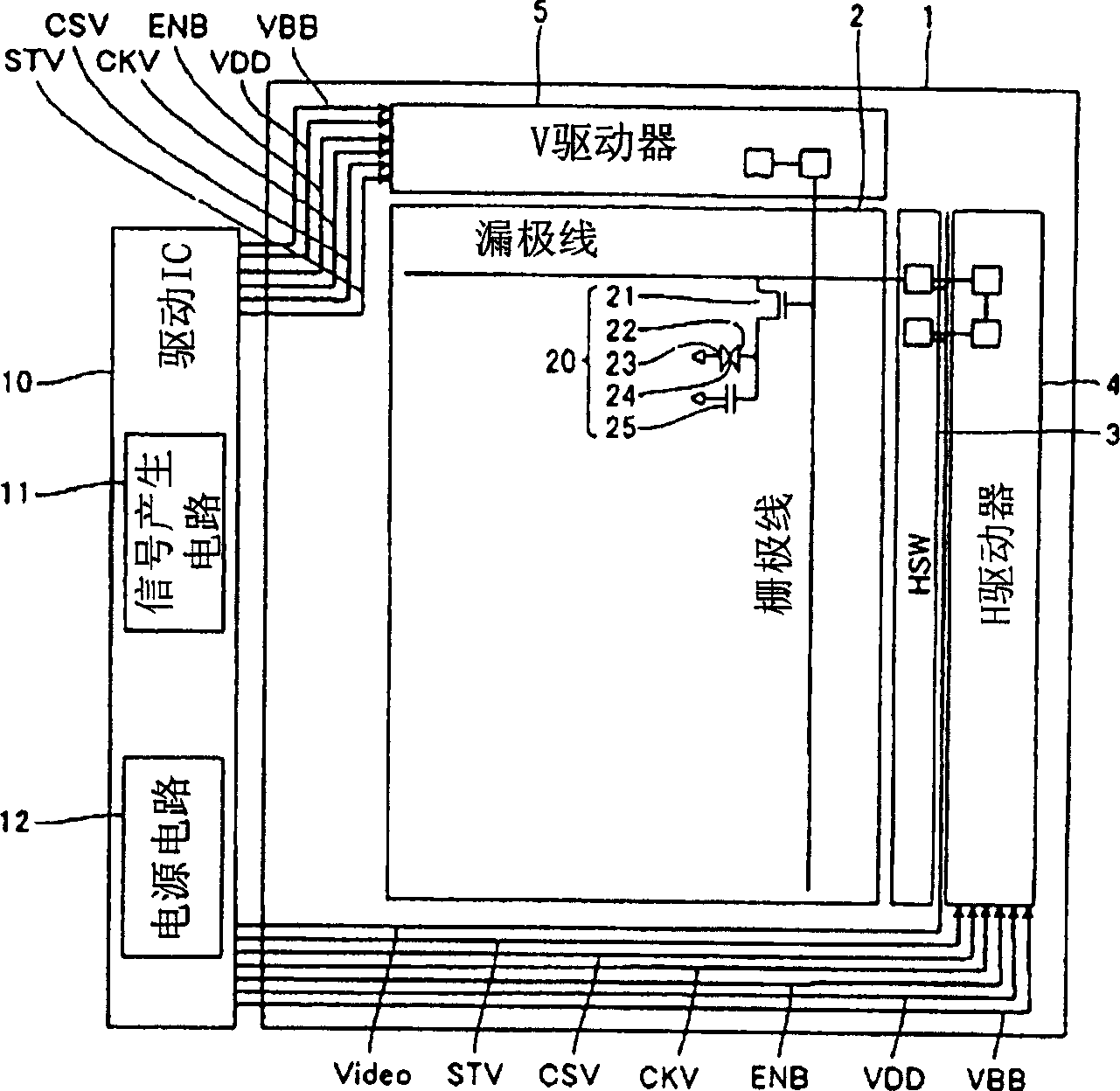
[0111] First refer to figure 1 , in this first embodiment, the display portion 2 is provided on the substrate 1 . In the display unit 2 , pixels 20 are arranged in a matrix. exist figure 1 In , only one pixel 20 is shown in order to simplify the drawing. Each pixel 20 is composed of: an n-channel transistor 21 (hereinafter referred to as a transistor 21), a pixel electrode 22, an opposite electrode 23 common to each pixel 20 arranged opposite to the pixel electrode 22, and surrounded by the pixel electrode 22 and the opposite electrode. The liquid crystal 24 between the electrodes 23 and the storage capacitor 25 constitute. The source of the transistor 21 is connected to the pixel electrode 22 and the storage capacitor 25 , and the drain is connected to the drain line. The gate of this transistor 21 is connected to a gate line.
[0112] Further, a horizontal switch (HSW) 3 and an H driver 4 for driving (scanning) a drain line of the display unit 2 are provided on the su...
no. 2 Embodiment
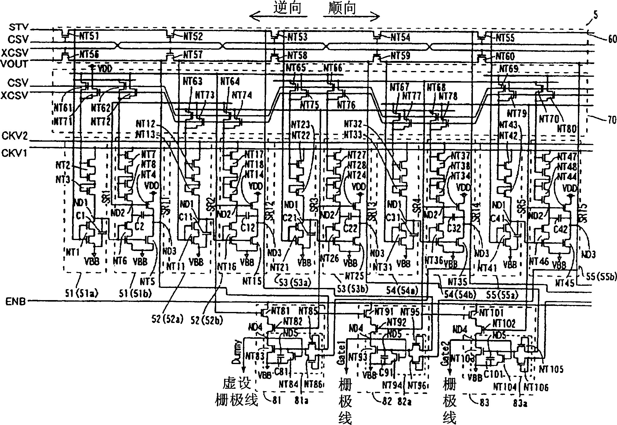
[0203] The second embodiment has almost the same configuration as the first embodiment. refer to Figure 5 , differs from the first embodiment in that: inside the V driver 5a, multiple stages of shift register circuit sections 501 to 505, scanning direction switching circuit section 600, input signal switching circuit section 700, and multiple stages of The transistors in the logic synthesis circuit sections 801 to 803 are changed to p-channel transistors. exist Figure 5 In order to simplify the drawing, only 5 stages of shift register circuit sections 501 to 505 and 3 stages of logic synthesis circuit sections 801 to 803 are shown, but shift registers corresponding to the number of pixels are actually arranged. Circuit section and logic synthesis circuit section.
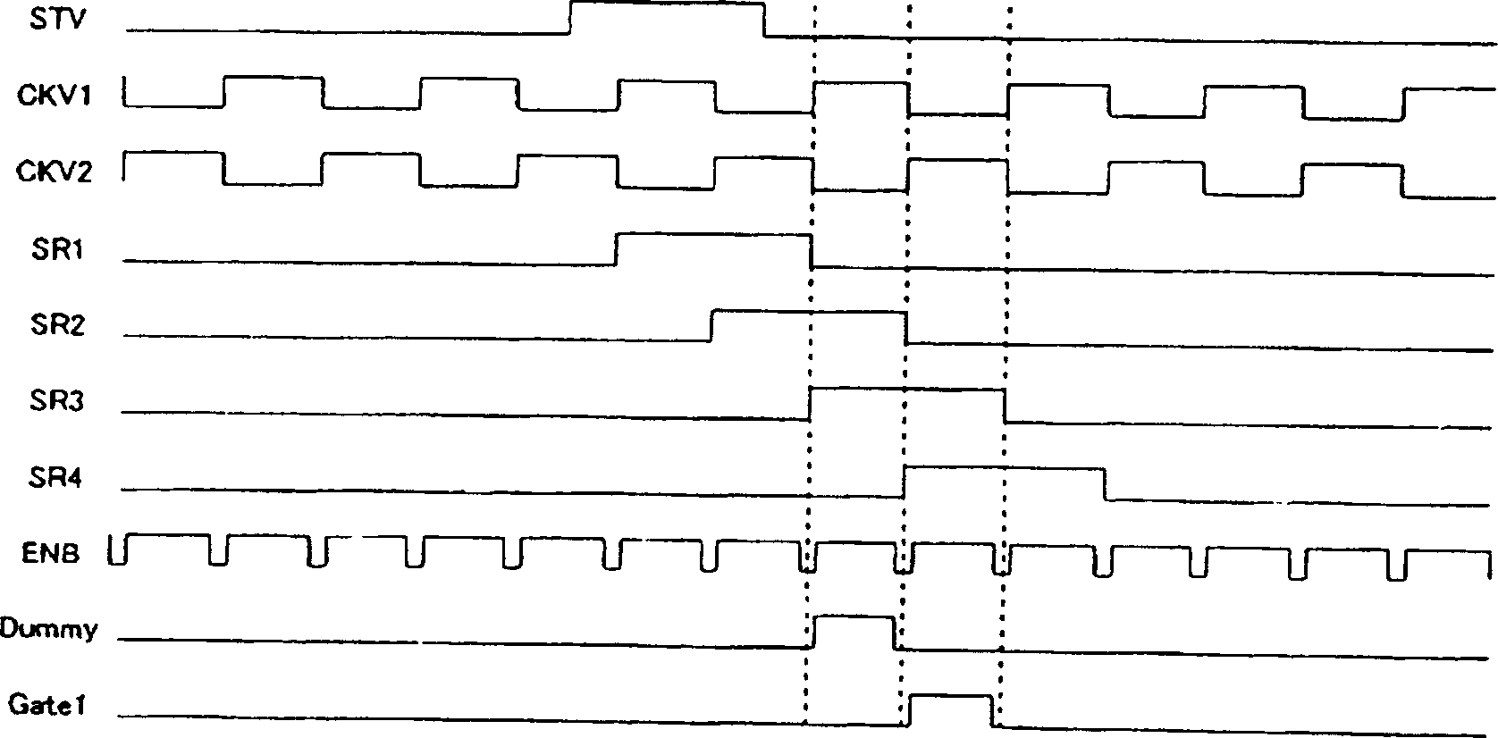
[0204] Next refer to Figure 5 and Figure 6 , the operation of the V driver 5a of the liquid crystal display device of the second embodiment will be described. In the V driver 5a of this second embodiment, ...
no. 3 Embodiment
[0207] refer to Figure 7 , in the third embodiment, in the configuration of the above-mentioned first embodiment, the drain of the transistor connected to the node outputting the shift output signal of the shift register circuit part after the third stage, the supply enable signal to replace the positive side potential case.
[0208] That is, if Figure 7 As shown, in the third embodiment, multi-stage shift register circuit units 511 to 515, scanning direction switching circuit unit 610, input signal switching circuit unit 710, and multi-stage logic synthesis circuit units 811 to 813 are provided. exist Figure 7 In order to simplify the drawing, only 5 stages of shift register circuit sections 511 to 515 and 3 stages of logic synthesis circuit sections 811 to 813 are shown, but shift register circuits corresponding to the number of pixels are actually arranged. Department and Logic Synthesis Circuit Department.
[0209] In addition, the shift register circuit section 511...
PUM
 Abstract
Description
Claims
Application Information
 - R&D
- Intellectual Property
- Life Sciences
- Materials
- Tech Scout
- Unparalleled Data Quality
- Higher Quality Content
- 60% Fewer Hallucinations
Browse by: Latest US Patents, China's latest patents, Technical Efficacy Thesaurus, Application Domain, Technology Topic, Popular Technical Reports.
© 2025 PatSnap. All rights reserved.Legal|Privacy policy|Modern Slavery Act Transparency Statement|Sitemap|About US| Contact US: help@patsnap.com