LED device possessing position mark

A technology of light-emitting diodes and positioning marks, applied to electrical components, circuits, semiconductor devices, etc., can solve problems such as difficulties, difficulty in identification, production capacity and defect rate reduction, so as to reduce abnormal conditions, easy identification, increase production capacity and yield rate Effect

Inactive Publication Date: 2006-07-05
NAN YA PHOTONICS INC
View PDF0 Cites 2 Cited by
  • Summary
  • Abstract
  • Description
  • Claims
  • Application Information

AI Technical Summary

Problems solved by technology

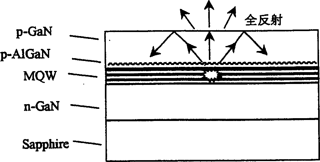
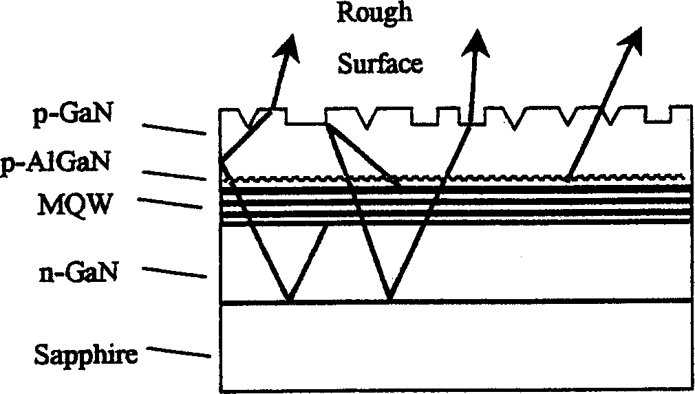
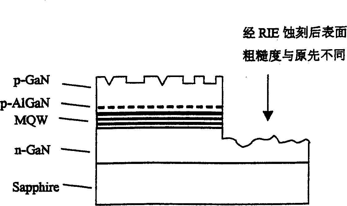
[0005] Although the roughening of the epitaxial surface can greatly improve the light extraction efficiency and increase the brightness of the LED, it will increase a lot of difficulties in the manufacturing process, especially in the sorting and packaging of the crystal grains in the later stage. Die sorting machine mainly uses P pole metal pad and N pole metal pad as the identification point when picking up the grain. The method is to use red light as the light source. When the red light shines on the grain surface, the CCD captures the image. When displayed on the LCD screen, the metal pads of the P electrode and the N electrode on the grain will appear white. When the color difference between the metal pads of the two electrodes is within the set range, the grain sorter can be used as a benchmark for identification, and The subsequent process is carried out, but when the epitaxial surface is too rough, a dry etching machine is required to etch the component to the n-GaN Layer (such as image 3 As shown), it is easy to make the roughness of the etched surface area different from that of the unetched surface. As a result, when the P pole metal pad and the N pole metal pad are evaporated on the component, it is easier to see on the stereo microscope or LCD screen There are black and white pads generated (eg Figure 4 As shown) or the color difference between the two is too large, or even due to the remaining needle probe traces on the metal pad, the grain sorter cannot be identified or the identification is difficult, resulting in abnormal occurrences or reduced production capacity;
[0006] From the above description, it can be found that in the traditional die sorting machine, die bonding machine and wire bonding machine, the die identification method of P pole metal pad and N pole metal pad is common due to design and process problems. There are problems that are not easy to identify, resulting in a decrease in production capacity and an increase in the defect rate. In other words, if a positioning device for easy identification in the die manufacturing process can be developed, the speed and accuracy of identification can be improved, thereby improving the overall quality. production capacity and reduce the generation of defective products

Method used


Image

  • LED device possessing position mark
  • LED device possessing position mark
  • LED device possessing position mark

Examples


Embodiment

[0026] In addition, the two alignment marks 51, 52 of the positioning device 50 are different according to the positions of the N-pole metal pad 20 and the P-pole metal pad 30, for example, when the N-pole metal pad 20 and the P-pole metal pad 30 of the die 10 When the relative position is side to side, the two alignment marks 51,52 of the positioning device 50 can be corner to corner (such as Figure 5 shown) or corner-to-edge (as in Image 6 shown) or side-to-side (as shown Figure 7 shown) position; and when the relative position of the N-pole metal pad 20 and the P-pole metal pad 30 of the crystal grain 10 is corner-to-side, the two alignment marks 51, 52 of the positioning device 50 can be corner-to-corner ( Such as Figure 8 shown) or corner-to-edge (as in Figure 9 shown) or side-to-side (as shown Figure 10 shown) position; in addition, when the relative position of the N-pole metal pad 20 and the P-pole metal pad 30 of the crystal grain 10 is at a corner-to-corner...


PUM


Abstract

Two opposite position marks are designed for procedure of fabricating crystal grain of light emitting diode. The two opposite position marks are located at same metal plane. The two opposite position marks can be setup in modes of corner-to-corner, or corner-to-edge, or edge-to-edge. Since two marks are located at same metal plane, their surface roughness is similar. Thus, device for fabricating crystal grain can recognize them easily. Selecting crystal grain effectively, the invention reduces unusual condition from happening greatly so as to raise integrated capacity and ration of fine products.

Description

technical field [0001] The invention relates to a light emitting diode, in particular to a light emitting diode device with positioning marks. Background technique [0002] In recent years, due to the successful development of blue light diodes, the three primary colors of light-emitting diodes have been completed, and large-scale outdoor full-color display boards have been realized. Due to the short wavelength of light emitted by blue light laser diodes, it can increase the data storage density (up to 25GB). It is an extremely important light source in the optical information system; [0003] As far as technology is concerned, red light, orange light, yellow light or yellow light emitting diode technologies in the visible light range have been quite mature and commercialized, while blue light diodes of the Nitride system have been developed, but the traditional In the GaN LED component structure, the light from the light-emitting layer cannot be effectively extracted from ...

Claims


Application Information

Patent Timeline
Patent Type & Authority Applications(China)
IPC IPC(8): H01L33/00
Inventor 王瑞瑜方博仁洪详竣苏崇智
Owner NAN YA PHOTONICS INC
Why Eureka
Try Eureka