Measuring apparatus

A kind of measuring equipment and equipment technology, which is applied in the direction of measuring devices, semiconductor/solid-state device testing/measurement, and material analysis using microwave means, which can solve problems such as instability, increased manufacturing costs of polishing pads, and inability to reach semiconductor wafers, etc., to achieve Effect of manufacturing cost reduction

Inactive Publication Date: 2006-07-19
EBARA CORP
View PDF0 Cites 25 Cited by
  • Summary
  • Abstract
  • Description
  • Claims
  • Application Information

AI Technical Summary

Problems solved by technology

[0007] However, the above measuring apparatus has the following problem: If an obstacle such as a polishing pad exists between the light source and the semiconductor wafer, the laser beam and visible light emitted from the light source cannot reach the semiconductor wafer
As a result, the number of manufacturing processes of the polishing pad increases, and thus the manufacturing cost of the polishing pad as a consumable component increases
In addition, in the above measuring equipment, the laser beam reflected from the semiconductor wafer and the reflected visible light are unstable
Therefore, it is difficult to accurately measure film thickness

Method used


Image

  • Measuring apparatus
  • Measuring apparatus
  • Measuring apparatus

Examples


Embodiment Construction

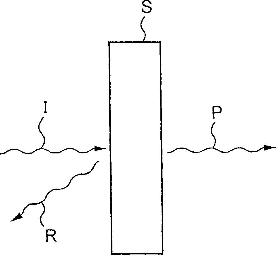
[0041] A measuring device according to an embodiment of the present invention will be described below with reference to the accompanying drawings. Figure 1A is a schematic diagram showing the principle of the measuring device according to the first embodiment of the present invention. Such as Figure 1A As shown, when microwaves (incident waves) are transmitted to the object S to be measured, the microwaves are reflected by the object S. Microwaves reflected from the object S (hereinafter referred to as reflected waves R) have amplitudes and phases that vary with the structure and physical properties of the object S such as thickness and the like. Therefore, the structure of the object S can be analyzed by detecting at least one of the amplitude and the phase of the reflected wave R. The structure of an object includes object thickness, internal defects such as voids formed in the object, permittivity, electrical conductivity, and magnetic permeability.

[0042] For example,...


PUM

PropertyMeasurementUnit
thicknessaaaaaaaaaa

Abstract

The present invention relates to a measuring apparatus for measuring a thickness or the like of a thin film formed on a surface of a substrate such as a semiconductor wafer. The measuring apparatus includes a microwave emission device (40) for emitting a microwave to a substance , a microwave generator (45) for supplying the microwave to the microwave emission device (40), a detector (47) for detecting an amplitude or a phase of the microwave which has been reflected from or passed through the substance, and an analyzer (48) for analyzing a structure of the substance based on the amplitude or the phase of the microwave which has been detected by the detector (47).

Description

technical field [0001] The present invention relates to a measuring device for measuring the thickness, etc. of an object, and more particularly, to a measuring device for measuring the thickness, etc., of a film formed on the surface of a substrate such as a semiconductor wafer. Background technique [0002] As semiconductor devices have become more and more highly integrated in recent years, circuit interconnections are required to be finer, and the number of layers of multilayer interconnections has increased. In this trend, planarization of the surface of a substrate such as a semiconductor wafer is required. Specifically, as circuit interconnections become thinner, the wavelength of light used in photolithography becomes shorter. In the case of using light with a short wavelength, the allowable step height in the focal area of ​​the substrate surface becomes smaller. Therefore, the substrate requires a very flat surface so that the step heights of the focal regions be...

Claims


Application Information

Patent Timeline
Patent Type & Authority Applications(China)
IPC IPC(8): G01B15/02G01N22/02H01L21/66G01N22/00
CPCG01N22/00G01B15/02G01N22/02H01L22/00
Inventor 多田光男须藤康成
Owner EBARA CORP
Why Eureka
Try Eureka