Field programmable gate array loading method

A gate array and programming logic technology, applied in program control devices, instruments, electrical digital data processing, etc., can solve the problems affecting the system startup speed, long chip selection effective time, long loading time, etc., to reduce fault recovery time, Reduce startup time, improve product performance and metrics

Inactive Publication Date: 2006-07-26
HUAWEI TECH CO LTD
View PDF1 Cites 13 Cited by
  • Summary
  • Abstract
  • Description
  • Claims
  • Application Information

AI Technical Summary

Problems solved by technology

However, since the time for reading and writing FLASH is generally longer, the effective time of chip selection for each access to the EPLD register should also be longer
Moreover, the general data is loaded from the EPLD to the FPGA according to each BIT operation. When using this method to load, each time a BIT is loaded, the EPLD wil

Method used


Image

  • Field programmable gate array loading method
  • Field programmable gate array loading method
  • Field programmable gate array loading method

Examples


Embodiment Construction

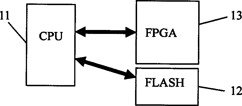
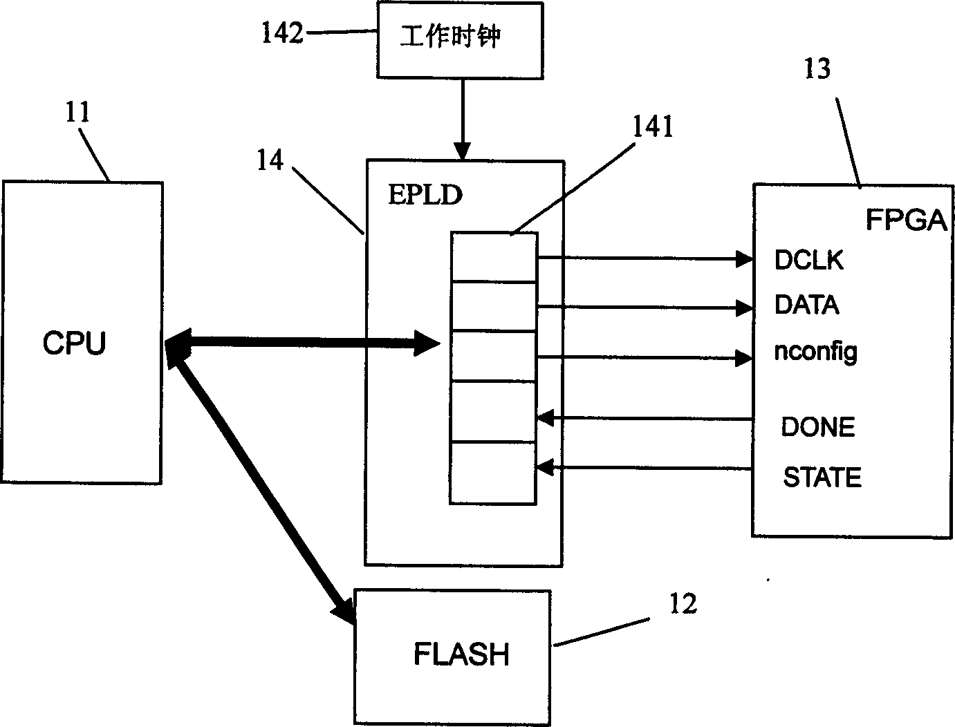
[0031] see Figure 4 to Figure 6 , is a preferred embodiment of the loading method of the field programmable gate array of the present invention, first as follows Figure 4 An erasable programmable logic device EPLD14 is provided between the CPU 11 and the field programmable array FPGA 13 . The CPU 11 is connected to the EPLD 14 and the FLASH 12 through a bus, so that the files to be loaded stored in the FLASH 12 can be quickly loaded into the FPGA 13 through the EPLD 14. The EPLD 14 is provided with a control register 31 , an 8-bit load data register 32 and a clock output logic 33 , and an external operating clock 142 is added to the EPLD 14 . The control register 31 is connected with the control signal pins (nCONFIG, DONE, STATE) of the FPGA13, the load data register 32 is connected with the data input pin of the FPGA13, and the clock output logic 33 is connected with the clock input pin of the FPGA13. connect.

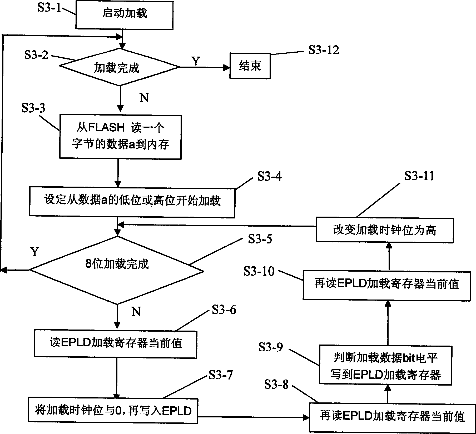
[0032] like Figure 5 As shown, when the loading needs to ...


PUM


Abstract

Disclosed is a method for loading field programmable gate array, which comprises steps of: placing EPLD between CPU and FPGA; S5-1: starting to load; S5-2: detecting whether the loading is over or not, that is, stopping loading by judging the DONE signal of FPGA as end, and when judging the DONE signal of being not over, executing following steps: S5-3íóS5-4: Writing one byte data needed for loading into the loading data register of the EPLD once by CPU; S5-5: completing the loading of needed data to the FPGA by the internal logic of the EPLD; S5-6: delaying some time; repeating the S5-2 to S5-6 until finishing loading.

Description

technical field [0001] The invention relates to a method for loading files into field-programmable gate arrays (FPGA, field-programmable gate arrays), in particular to a method for loading files into FPGA by using an erasable programmable logic device (EPLD, erasable programmable logic device). Background technique [0002] A Field Programmable Gate Array (FPGA) is an erasable programmable read-only memory. Usually, when the board is powered on and initialized, relevant programs and data are loaded into the FPGA. After the FPGA is initialized, complex logic control can be completed to realize various business processing functions. Since FPGA is a logic chip that does not save data when power is off, it is required to be reloaded every time it is powered on, that is, to rewrite data into the FPGA chip so that it can work normally. [0003] name meaning nCONFIG Logic chip reset pin nSTATUS Logic chip reset complete status pin DONE ...

Claims


Application Information

Patent Timeline
IPC IPC(8): G06F9/44G06F12/00
Inventor 祝文刚
Owner HUAWEI TECH CO LTD
Why Eureka
Try Eureka