Printed circuit board and formation method

A technology of printed circuit boards and substrates, which is applied in the direction of printed circuits, printed circuit manufacturing, printed circuit components, etc., and can solve problems such as unevenness of the front of printed circuit boards, inability to fully absorb solder, holes and overflowing glue, etc.

Inactive Publication Date: 2006-08-09
LITE ON OPTO TECH (CHANGZHOU) CO LTD +1
View PDF0 Cites 10 Cited by
  • Summary
  • Abstract
  • Description
  • Claims
  • Application Information

AI Technical Summary

Problems solved by technology

However, this method also has its limitations, that is, when the aperture of the via hole is too small, the end on the back side may not be able to fully absorb the solder; and when the aperture of the via hole is too large

Method used


Image

  • Printed circuit board and formation method
  • Printed circuit board and formation method
  • Printed circuit board and formation method

Examples


Embodiment Construction

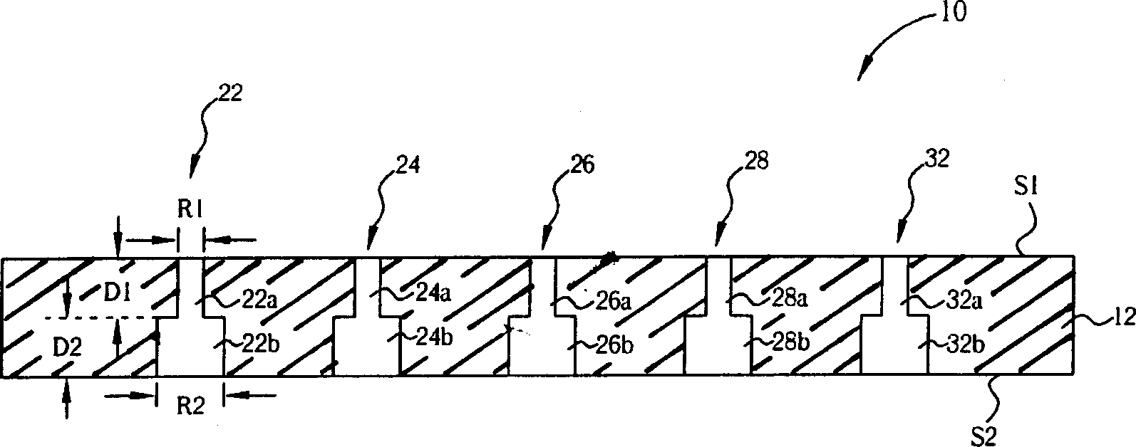
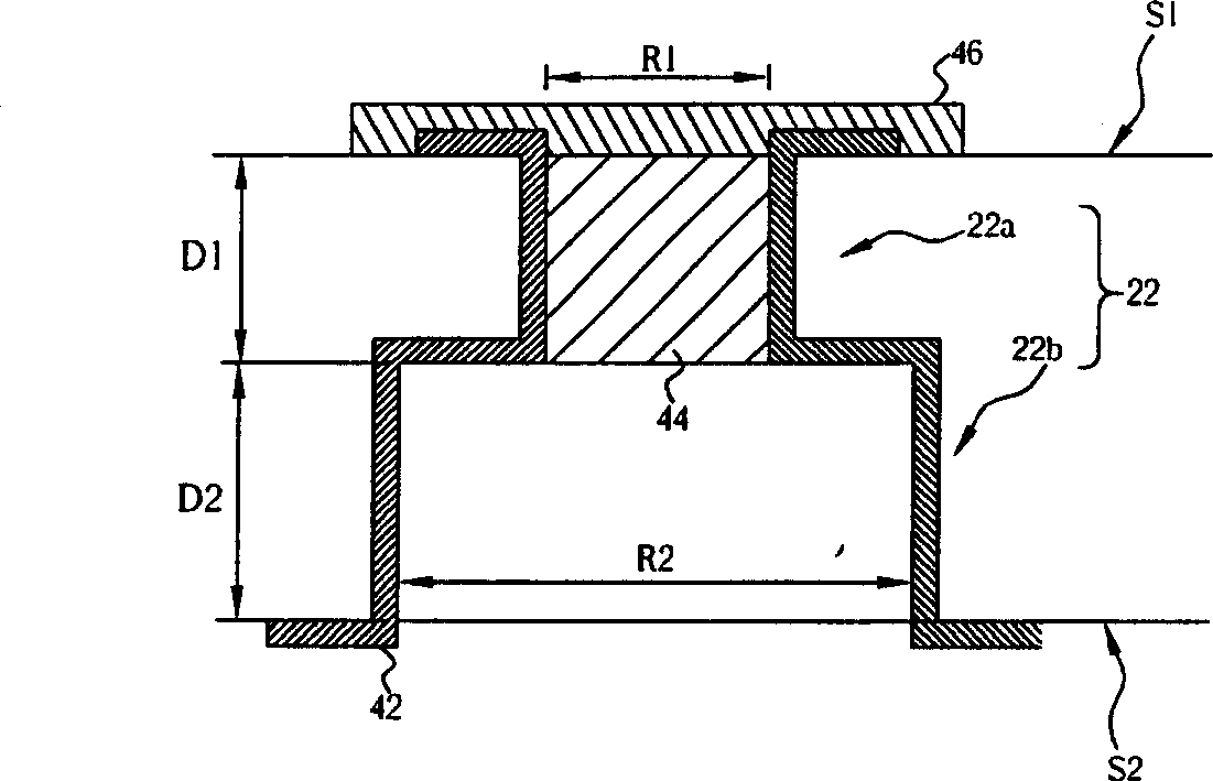
[0020] see figure 1 , figure 1 It is a sectional view of an embodiment of the printed circuit board 10 of the present invention. In this embodiment, the printed circuit board 10 includes a substrate 12 and a conductive layer. The substrate 12 has a surface S1 , a surface S2 and a plurality of through holes 22 , 24 , 26 , 28 , 32 . The through holes 22, 24, 26, 28, 32 can be divided into upper and lower parts according to their diameters, which are respectively 22a and 22b, 24a and 24b, 26a and 26b, 28a and 28b, 32a and 32b. And the upper half 22a, 24a, 26a, 28a, 32a of the through holes 22, 24, 26, 28, 32 in this embodiment all have the same diameter R1 and depth D1, and the through holes 22, 24, 26, 28, The lower halves 22b, 24b, 26b, 28b, 32b of 32 all have the same diameter R2 and depth D2, and the diameter R2 is larger than the diameter R1. In addition, the function and style of the conductive layer will be described in detail below.

[0021] see figure 2 , figure...


PUM


Abstract

The printing circuit board (PCB) includes a base plate and conducting layers. There are through holes on the base plate. First aperture of the through holes is located at one side; and second aperture of the through holes is located at another side; the second aperture is larger than the first aperture. Being setup on walls of through holes, conducting layers are in use for connecting two sides of base plate electrically. Obstruct material are plugged to one side of through holes on PCB; and the other side of through holes are kept unobstructed state in order to adsorb metal conductor in melting state. Cooled melted metal is attached to conducting layer tightly in order to fix PCB on electronic equipment. The said obstruct material prevents any liquid matter from flooding to another surface form one surface in fabrication process.

Description

【Technical field】 [0001] The invention relates to a printed circuit board and its forming method, in particular to a printed circuit board with a through hole and its forming method. 【Background technique】 [0002] The printed circuit board is an indispensable component in the electronics industry, and it can be applied to a mother board of an electronic product to mount other electronic components and provide wiring for other electronic components. Alternatively, the printed circuit board can also be used as an adapter for a semi-finished product to fix the semi-finished product on the main board. The conventional process steps of printed circuit boards include drilling, electroplating, circuit etching, pressing, solder resist treatment and tin spraying, etc. When the printed circuit board is used as an interposer board, one of the application methods is to drill and plate on the interposer board to create a via hole to electrically connect the circuit on the front of the ...

Claims


Application Information

Patent Timeline
IPC IPC(8): H05K1/02H05K3/00
Inventor 林勇任
Owner LITE ON OPTO TECH (CHANGZHOU) CO LTD
Why Eureka
Try Eureka