Semiconductor component and its forming method

A semiconductor and component technology, applied in the field of improved shallow trench isolation, can solve problems such as defects, shallow trench isolation sidewall damage, stress-induced defects, etc., to suppress corner parasitic transistors, reduce channel stress, and reduce silicide Effects of Inducing Joint Problems

Active Publication Date: 2006-09-27
TAIWAN SEMICON MFG CO LTD
View PDF0 Cites 6 Cited by
  • Summary
  • Abstract
  • Description
  • Claims
  • Application Information

AI Technical Summary

Problems solved by technology

While this conventional filleting process system can fillet the corners, it still has potential drawbacks. One disadvantage of this conventional filleting process is that it creates stress-induced defects that can be problematic for today's shrinking component geometries.
Another potential disadvantage is STI sidewall damage caused by the high density plasma (HPD) oxide trench filling process that forms the oxide substrate layer
Another disadvantage is the divot-induced reverse narrow channel effect (RNCE) induced by the breakage of the corner-edge parasitic transistors. caused by the place

Method used


Image

  • Semiconductor component and its forming method
  • Semiconductor component and its forming method
  • Semiconductor component and its forming method

Examples


Embodiment Construction

[0054] Although a novel shallow trench isolation structure fabrication process of the present invention that promotes active region isolation, device yield, and reliability of structures is illustrated and described in detail below, the details presented are not intended to be limiting. In the present invention, various modifications and structural changes can be made without departing from the spirit of the present invention.

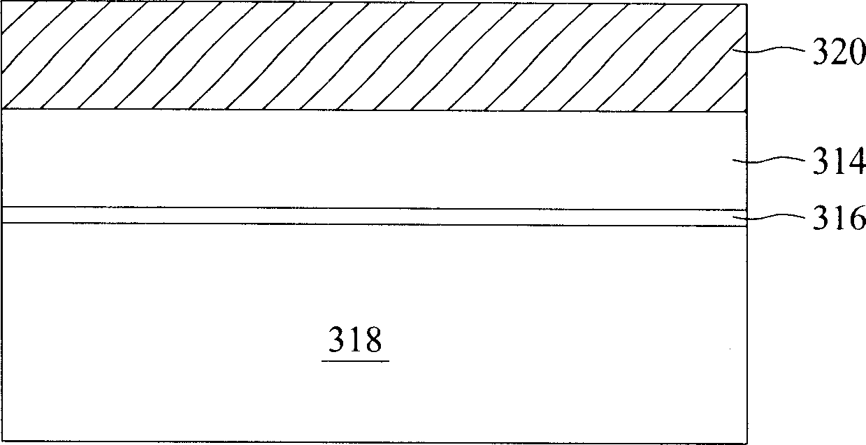
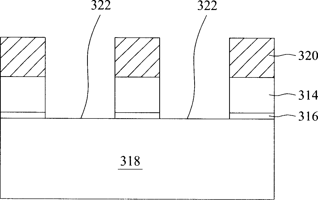
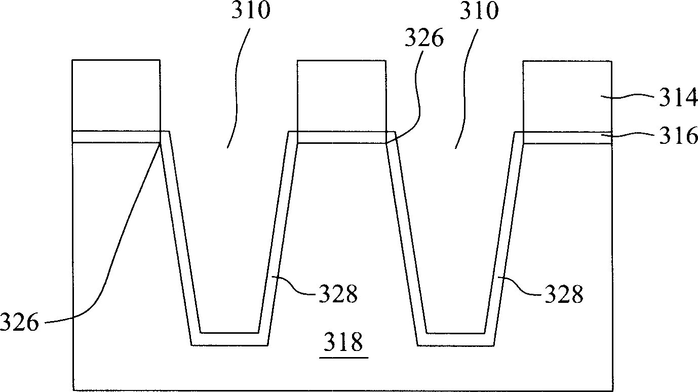
[0055] Please refer to Figure 1A to Figure 1D , which illustrates a conventional STI manufacturing process. Such as Figure 1A As shown, the silicon monoxide layer 316 is formed on a substrate material 318, which may be silicon, silicon-on-insulator (SOI), germanium, carbon, or a group thereof. The silicon oxide layer 316 can be formed by oxidizing a silicon substrate through a thermal oxidation process, a chemical vapor deposition (CVD) or other applicable techniques. Then, a silicon nitride layer 314 is formed on the silicon oxide layer 316 by an ...


PUM


Abstract

A method and system for isolation trenches includes forming isolation trenches in a semiconductor substrate, filling the trenches with a filler material, creating voids near top edges of the trenches and annealing by a gaseous ambient to reflow the edges of the trenches causing the edges to become rounded and overhang the trench. The filler material may be a dielectric. Transistors are then formed in close proximity to the trenches and may include source / drain regions formed in the rounded portion of the semiconductor substrate that overhangs the trench.

Description

technical field [0001] The present invention relates to a manufacturing method of a semiconductor device, and in particular to an improved manufacturing process of a shallow trench isolation (STI) structure. Background technique [0002] Semiconductor devices can use isolation structures to isolate electrical properties between different components. The isolation structures between the various components of the semiconductor device can reduce harmful interference effects that may cause device performance to decrease. As long as the components are isolated from each other, an electrical path can be established between the components of the semiconductor device to obtain ideal electrical properties. [0003] The conventional method for manufacturing the semiconductor device isolation structure generally utilizes a local oxidation of silicon (LOCOS) process. In the LOCOS process, an oxidation mask is used to provide a pattern and a field oxide layer is thermally grown. However...

Claims


Application Information

Patent Timeline
Patent Type & Authority Applications(China)
IPC IPC(8): H01L27/04H01L21/762
CPCH01L29/66636H01L21/823481H01L29/7834H01L21/76232H01L29/0847
Inventor 柯志欣葛崇祜黄健朝
Owner TAIWAN SEMICON MFG CO LTD
Why Eureka
Try Eureka