

Illumination system for a microlithography projection exposure installation
A lighting system and exposure system technology, applied in the field of lighting systems, can solve problems such as complex structures
- Summary
- Abstract
- Description
- Claims
- Application Information
AI Technical Summary
Problems solved by technology
Method used
Image

Examples
Embodiment Construction
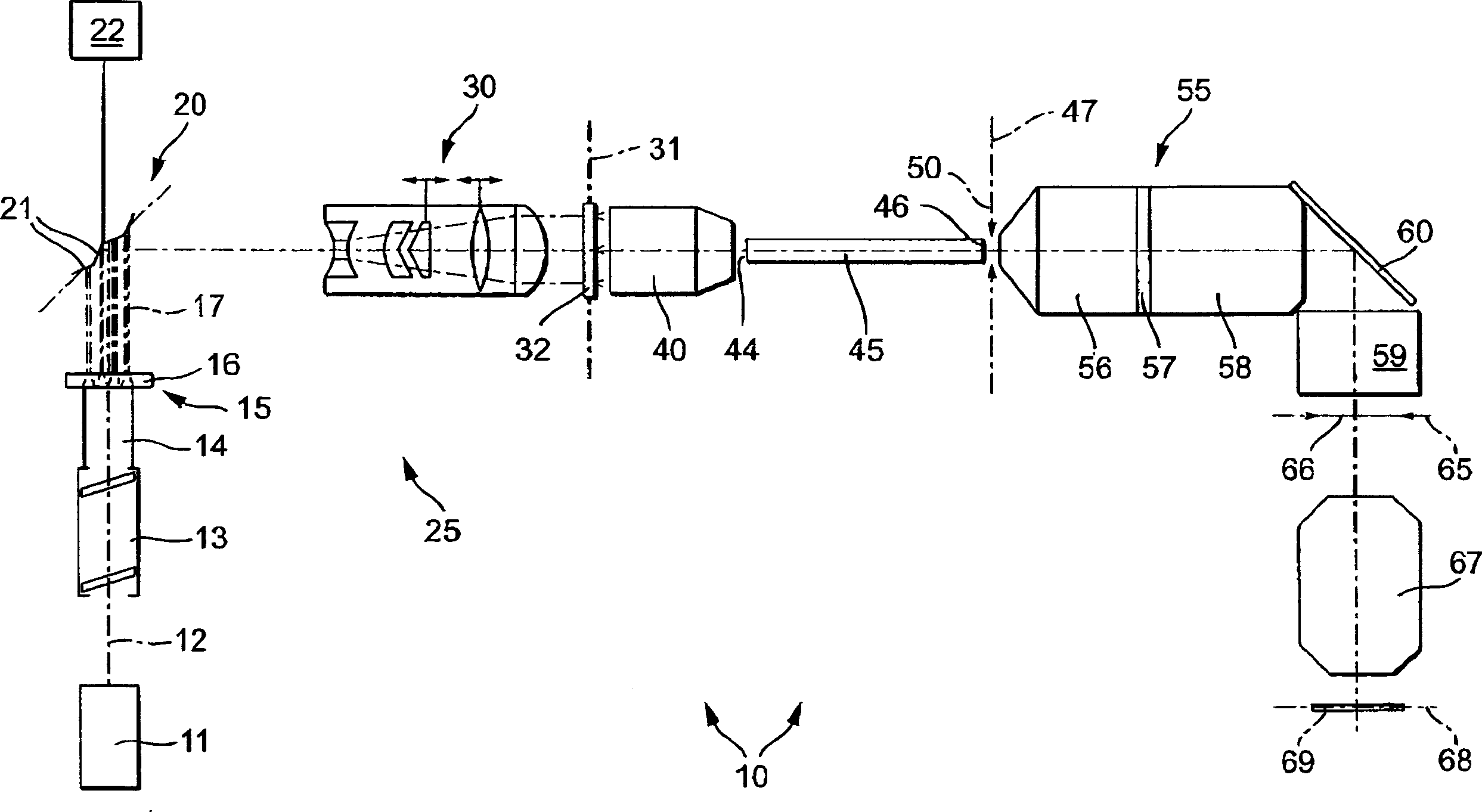
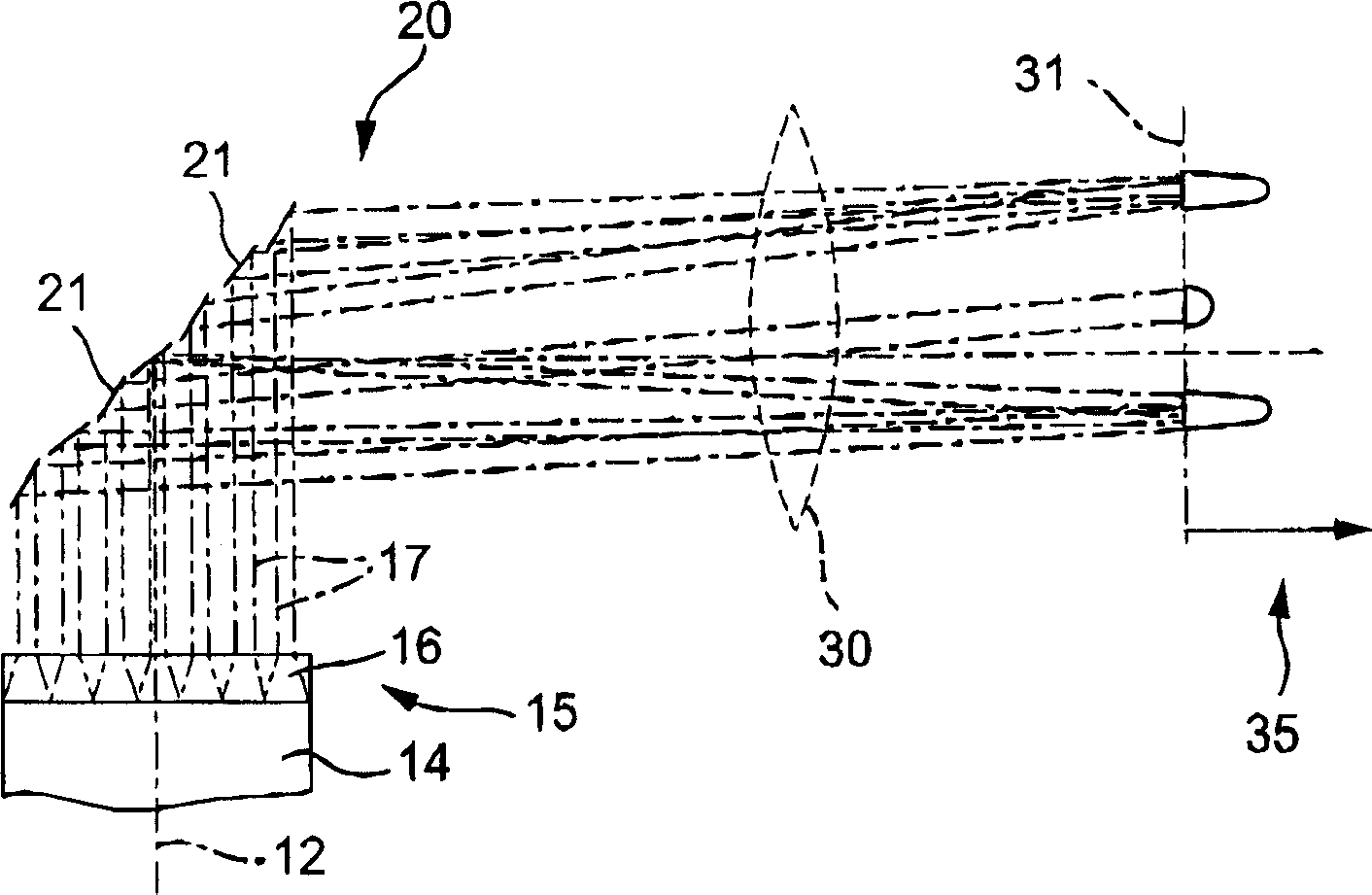
[0044] figure 1 Shows an example of an illumination system 10 for a projection exposure system for microlithography, which may be used in the production of semiconductor components or other fine structure components, and in order to achieve a resolution down to the micron level, the projection exposure system utilizes Operate with light in the deep ultraviolet range. The light source used is F 2 An excimer laser, which operates at a wavelength of approximately 157 nm, has a beam aligned coaxially with respect to the optical axis 12 of the illumination system. Similarly, other ultraviolet light sources can be used, such as an ArF excimer laser with a working wavelength of 193 nm, a KrF excimer laser with a working wavelength of 248 nm, or a mercury vapor lamp with a working wavelength of 365 nm or 436 nm, or a low wavelength light source at 157 nm.
[0045] The light from the light source 11 is first incident in the beam expander 13, which broadens the laser beam and, from t...
PUM
 Abstract
Description
Claims
Application Information