Electro-optical display device and method for manufacturing same

An electro-optical display and manufacturing method technology, applied in semiconductor/solid-state device manufacturing, circuits, electrical components, etc., can solve problems such as deviation, narrow selection of source/drain electrode materials, and difficulty in controlling the thickness of a-Si film. Effects of current suppression, simplification of manufacturing process, and prevention of deterioration of off-state characteristics

Inactive Publication Date: 2006-12-20
MITSUBISHI ELECTRIC CORP
View PDF2 Cites 1 Cited by
  • Summary
  • Abstract
  • Description
  • Claims
  • Application Information

AI Technical Summary

Problems solved by technology

[0015] However, in this method, it is necessary to etch the semiconductor film in the area of ​​hundreds of mm × hundreds of mm, and at the same time perform ashing of the photoresist in a very narrow area of ​​several μm to tens of μm and the underlying n + Therefore, it is difficult to control the film thickness of the a-Si film that becomes the channel part, and there is a problem of variation.
[0016] In addition, the source / drain electrodes are formed later, so a metal film material with etching selectivity relative to the a-Si film has to be used, and there is still the problem that the selection range of source / drain electrode materials is very narrow.

Method used


Image

  • Electro-optical display device and method for manufacturing same
  • Electro-optical display device and method for manufacturing same
  • Electro-optical display device and method for manufacturing same

Examples


Embodiment 1

[0076]

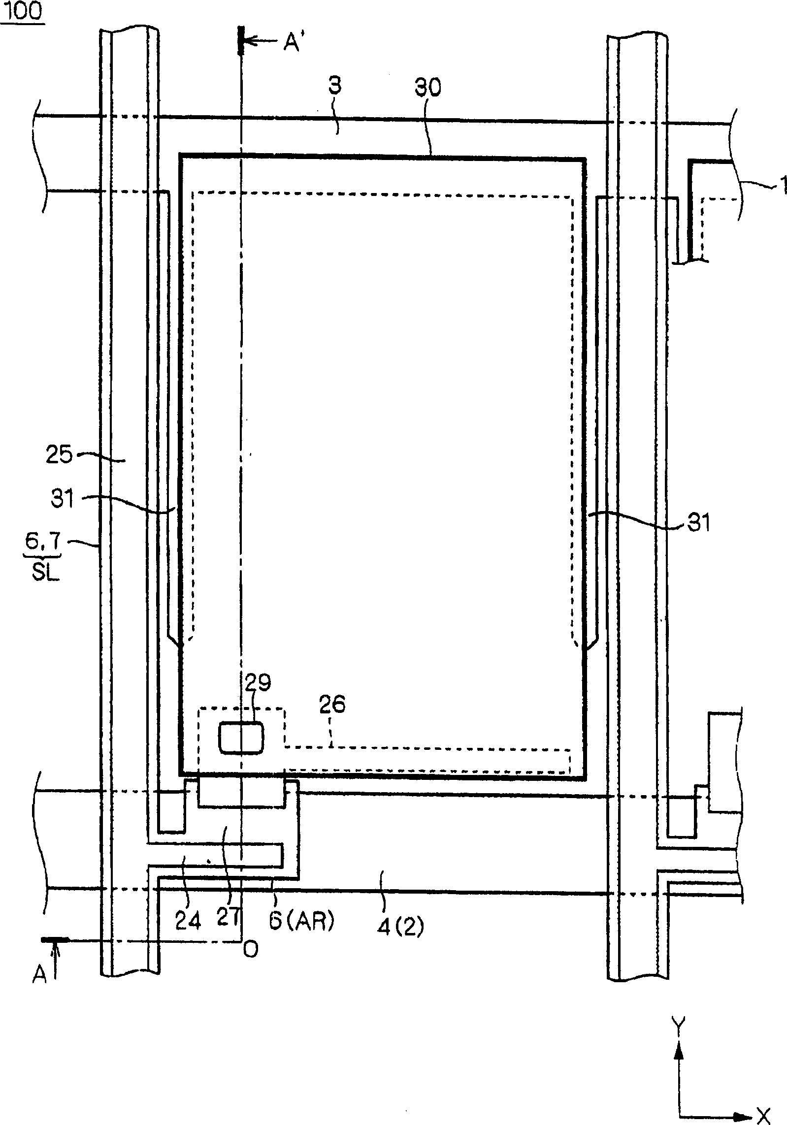
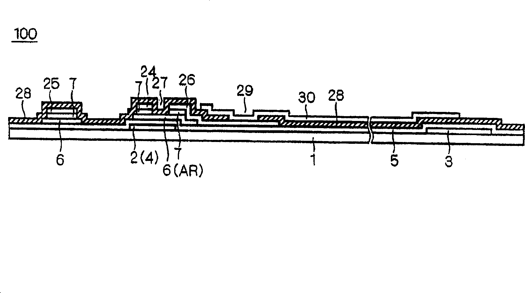
[0077] As the electro-optical display device of Embodiment 1 of the present invention, in figure 1 A planar structure of a TFT active matrix substrate 100 of a transmissive liquid crystal display device using TFTs as switching elements is shown, and, in figure 2 show figure 1 The cross-sectional structure on the line A-O-A' in the center.

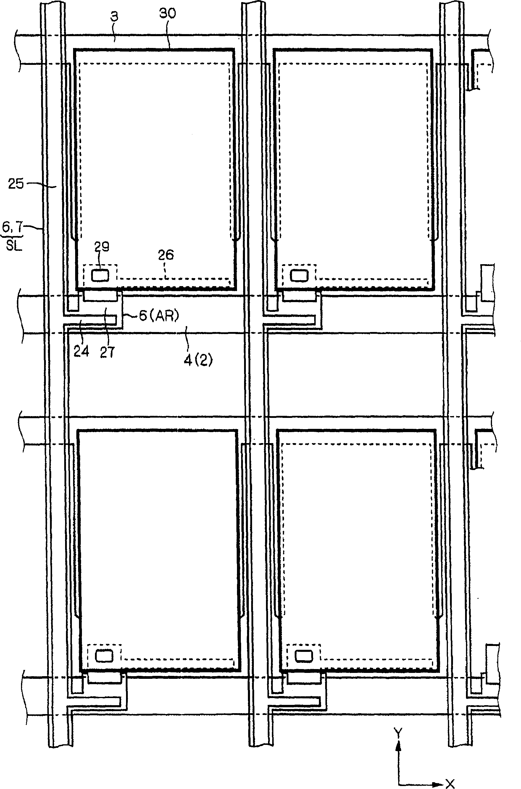
[0078] figure 1 It is a plan view showing one pixel on the TFT active matrix substrate 100, and a plurality of such pixels are arranged in a matrix on the TFT active matrix substrate 100.

[0079] Such as figure 1 As shown, on a transparent insulating substrate 1 such as a glass substrate, a gate wiring 4 partly constituting a gate electrode 2 is arranged. The gate wiring 4 is arranged so as to extend linearly in one direction on the transparent insulating substrate 1 , this direction is referred to as the X direction here, and the direction perpendicular to the X direction in a plane is referred to as the Y direction.

[0...

Embodiment 2

[0161]

[0162] As the electro-optical display device of Embodiment 2 of the present invention, in Figure 23 A planar structure of a TFT active matrix substrate 200 of a self-luminous organic EL display device equipped with an organic electroluminescent (EL) element using a TFT as a switching element is shown, and is shown in FIG. 24 Figure 23 The cross-sectional structure of the B-O-B' line in the middle.

[0163] Figure 23 It is a plan view showing one pixel on the TFT active matrix substrate 200, and a plurality of such pixels are arranged in a matrix on the TFT active matrix substrate 200. Also, in Figure 23 and Figure 24, for the figure 1 and figure 2 The same structure of the shown TFT active matrix substrate 100 uses the same symbols, and repeated descriptions are omitted.

[0164] Such as Figure 23 As shown, on a transparent insulating substrate 1 such as a glass substrate, a gate wiring 4 partly constituting a gate electrode 2 is arranged. The gate wiri...


PUM


Abstract

The present invention provides simplified manufacture process of TFT structure of different source electrode/drain electrode materials and one electro-optical display device capable of controlling the thickness of semiconductor film layer forming the TFT channels accurately for homogeneous display. The drain electrode is configured to extend from the active region to the transparent insulating substrate below the pixel electrode. The source electrode and the source wire are so configured that their ends are in the back of the semiconductor film, and the drain electrode on the active region has also end in the back of the semiconductor film.

Description

technical field [0001] The present invention relates to an electro-optical display device and a manufacturing method thereof, in particular to an active matrix electro-optical display device provided with a thin film transistor (TFT) as a switching element and a manufacturing method thereof. Background technique [0002] In electro-optic display devices using liquid crystal or organic EL (electroluminescence) as electro-optic elements, active matrix TFT arrays in which switching elements such as thin-film transistors are arranged in an array on a substrate and an independent image signal is applied to each display pixel are widely used. substrate. [0003] In order to improve the productivity of this kind of electro-optical display device, it is necessary to reduce the manufacturing process of the TFT array substrate. For example, patent document 1 discloses the technology of reducing the photoplate making process by referring to FIGS. Plate making process A method of manuf...

Claims


Application Information

Patent Timeline
Patent Type & Authority Applications(China)
IPC IPC(8): H01L27/12H01L21/84
Inventor 增田惠荒木利夫日野辉重
Owner MITSUBISHI ELECTRIC CORP
Why Eureka
Try Eureka