Electroluminescence device, method of manufacturing electroluminescence device, and electronic apparatus
An electroluminescence and manufacturing method technology, applied in electroluminescence light sources, lighting devices, electro-solid devices, etc., can solve the problems of reduced productivity, difficult step management, long etching time, etc., and achieves suppression of increased times and step management easy, avoid side effects
- Summary
- Abstract
- Description
- Claims
- Application Information
AI Technical Summary
Problems solved by technology
Method used
Image


Examples
no. 1 approach
[0099] (Basic structure of EL device)
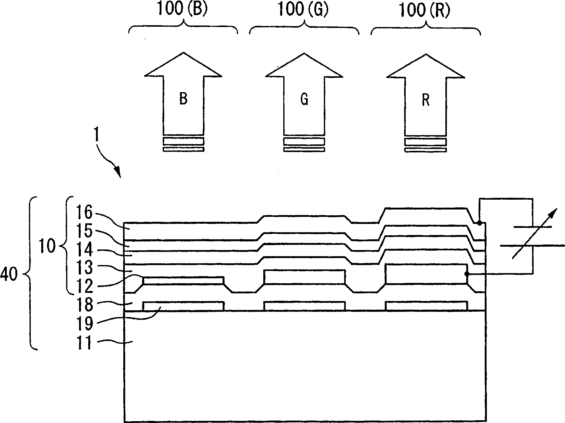
[0100] figure 1 It is a cross-sectional view schematically showing the structure of the organic EL device (EL device) according to the first embodiment of the present invention.
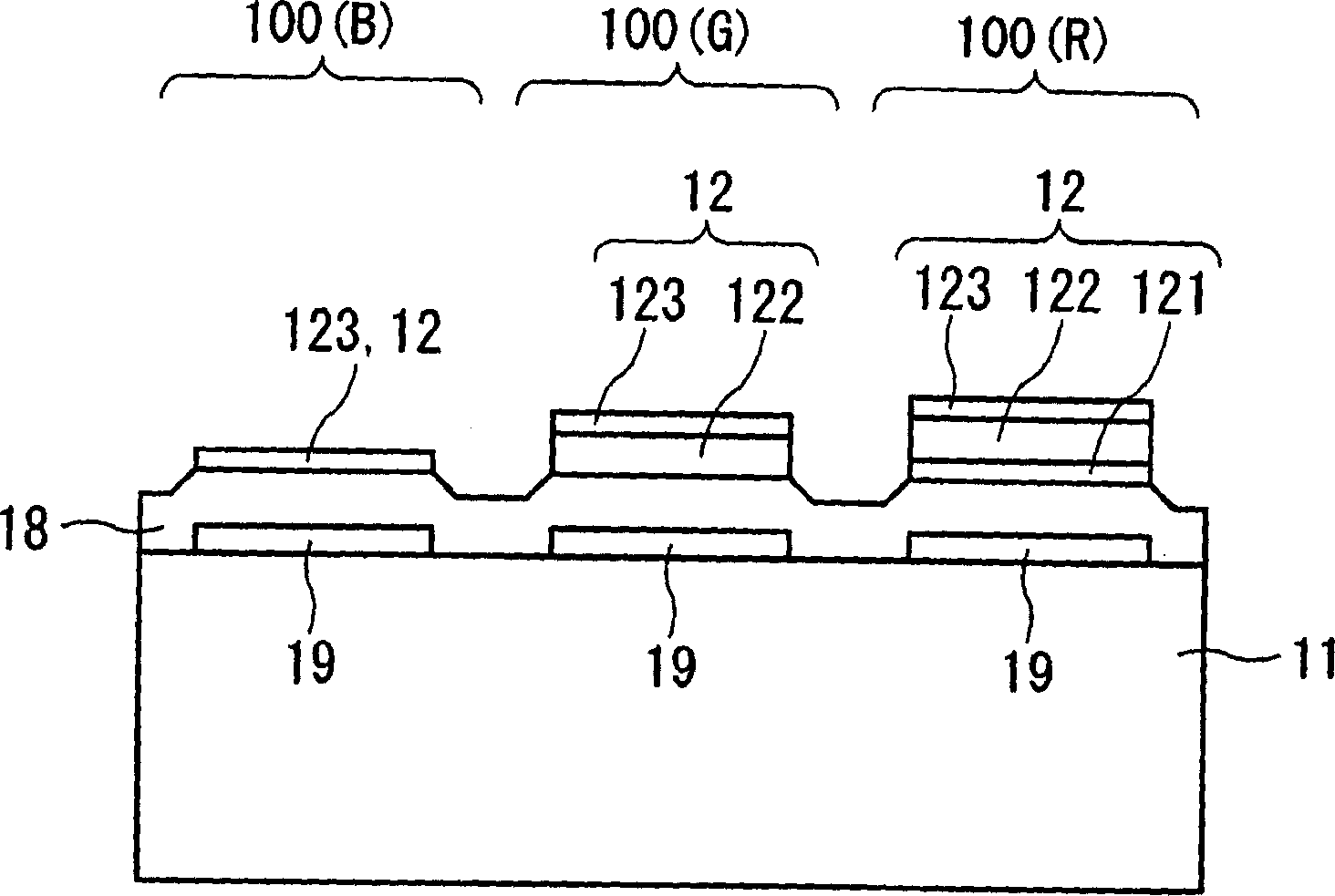
[0101] exist figure 1 Among them, the organic EL device of this embodiment is a top emission type device that emits display light to the side opposite to the substrate 11 side when viewed from the light emitting layer 14 . The organic EL device 1 has pixels 100(R), 100(G), and 100(B). The pixel 100 (R) emits red (R) light, the pixel 100 (G) emits green (G), and the pixel 100 (B) emits blue (B) light. The organic EL element 10 is formed on each of the pixels 100(R), 100(G), and 100(B).
[0102] The organic EL element 10 has a transparent anode 12 made of ITO, a hole transport layer 13, a light emitting layer 14, an electron transport layer 15, and a layer made of a magnesium-silver alloy, which are sequentially stacked on the upper layer side of a substrate ...
no. 2 approach
[0151] Figure 4 It is a cross-sectional view schematically showing the structure of an organic EL device (EL device) according to a second embodiment of the present invention.
[0152] Figure 4 The organic EL device 1 shown is a top emission type device that emits display light to the side opposite to the substrate 11 side when viewed from the light emitting layer 14 , as in the first embodiment. The organic EL element 10 is formed in each of the red (R) emitting pixel 100 (R), the green (G) emitting pixel 100 (G), and the blue (B) emitting pixel 100 (B). The organic EL element 10 has a transparent anode 12 made of ITO, a hole transport layer 13, a light emitting layer 14, an electron transport layer 15, and a magnesium-silver alloy that are sequentially stacked on the upper layer side of a substrate 11 made of glass. The structure of the cathode layer 16 is semitransparent and semireflective.
[0153] In addition, a reflective layer 19 (total reflection layer) made of al...
Embodiment approach
[0166] In the above-described embodiment, a top emission type that emits display light to the side opposite to the substrate 11 side is described as an example, but the present invention can also be applied to a bottom emission type that emits display light to the substrate side. That is, in the bottom emission type, a semi-transparent and semi-reflective lower layer side reflective layer is formed on the lower layer side of the anode, but if an insulating protective film is formed between the anode and the semi-transparent and semi-reflective lower layer side reflective layer, etching will form In the case of an anode, deterioration of the reflective layer on the lower layer side can be prevented.
[0167] In addition, in the above-mentioned embodiment, there are three layers such as the hole transport layer 13, the light emitting layer 14, and the electron transport layer 15 between the anode 12 and the cathode layer 16, but it is also possible to take a further layer between...
PUM
| Property | Measurement | Unit |
|---|---|---|
| Thickness | aaaaa | aaaaa |
| Film thickness | aaaaa | aaaaa |
| Thickness | aaaaa | aaaaa |
Abstract
Description
Claims
Application Information
 - R&D
- Intellectual Property
- Life Sciences
- Materials
- Tech Scout
- Unparalleled Data Quality
- Higher Quality Content
- 60% Fewer Hallucinations
Browse by: Latest US Patents, China's latest patents, Technical Efficacy Thesaurus, Application Domain, Technology Topic, Popular Technical Reports.
© 2025 PatSnap. All rights reserved.Legal|Privacy policy|Modern Slavery Act Transparency Statement|Sitemap|About US| Contact US: help@patsnap.com