

Photoelectric converter
A photoelectric conversion device and photoelectric conversion technology, applied in the coupling of optical waveguides, etc., can solve the problems of reduced reliability of OSA, uneven surface of contact parts, and reduced contact area, so as to improve shock resistance and thermal conductivity, and suppress electromagnetic interference , the effect of improving reliability
- Summary
- Abstract
- Description
- Claims
- Application Information
AI Technical Summary
Problems solved by technology
Method used
Image

Examples
Embodiment 1
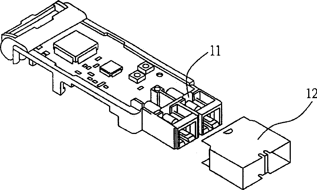
[0028] Figure 4 It is a structural schematic diagram of Embodiment 1 of the photoelectric conversion device of the present invention. As shown in the figure, the photoelectric conversion device 3 of the present invention at least includes: an optical sub-assembly (Optical Sub-Assembly; OSA) 31 , a circuit board 323 , a casing 32 and a conductive elastic interface unit 33 . The optical subassembly 31 is electrically connected to the circuit board 323 , which constitutes a signal processing module, and the optical subassembly 31 is equivalent to a photoelectric conversion assembly.
[0029] The optical sub-assembly 31 is an optical transmitting assembly (Transmitter Optical Sub-Assembly; TOSA) that converts electrical signals into optical signals and emits optical signals, or an optical receiving assembly for receiving optical signals and converting optical signals into electrical signals (Receive Optical Sub-Assembly; ROSA), or an optical transceiver assembly (Transmitter / Rec...
Embodiment 2
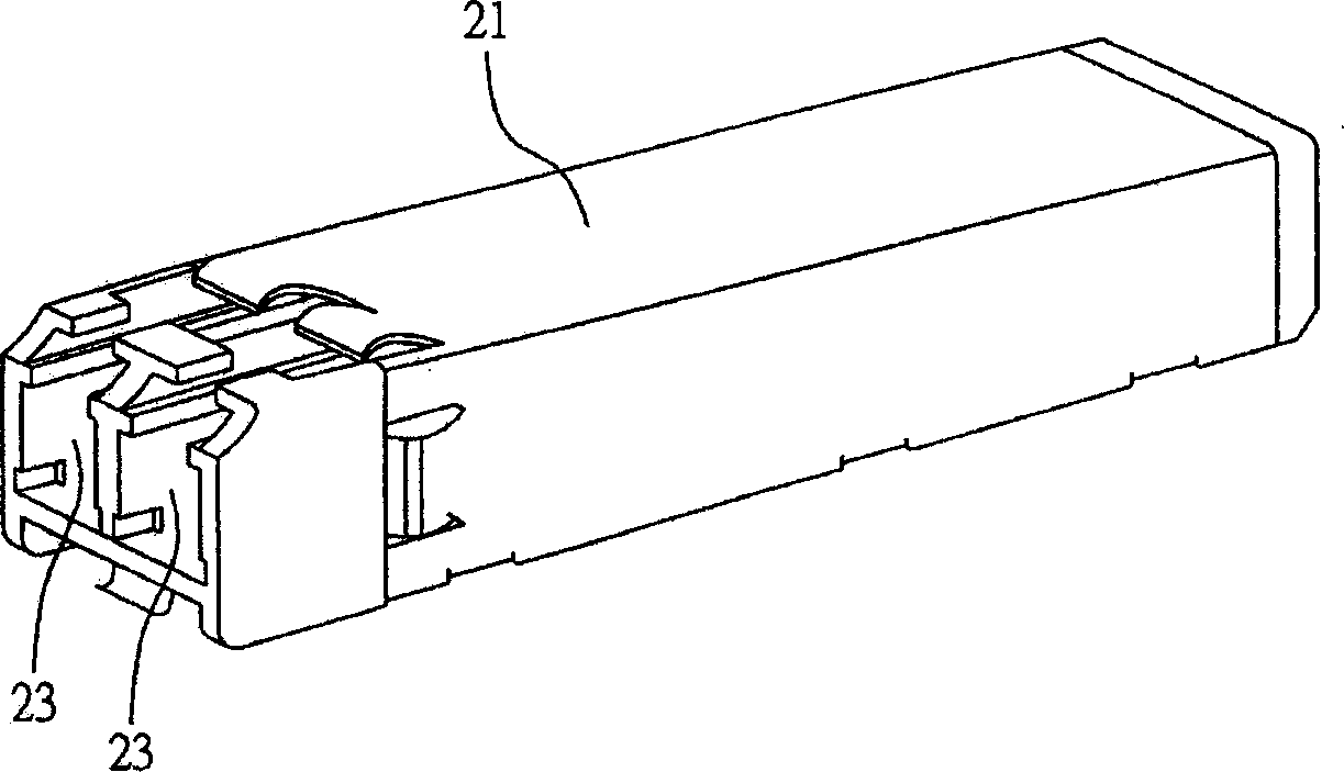
[0035] Figure 6 It is a schematic diagram of Embodiment 2 of the photoelectric conversion device of the present invention. As shown in the figure, the photoelectric conversion device 3 of Embodiment 2 is roughly the same as that described in Embodiment 1, except that the elastic interface unit 33 of Embodiment 2 It is composed of two conductive shrapnel 33a, 33b. Wherein the conductive elastic piece 33a is fixedly connected to the inner surface of the upper cover 321 and can also be integrally formed with the upper cover 321 ; the conductive elastic piece 33b is fixedly connected to the lower cover 322 and can also be integrally formed with the lower cover 322 . When the upper cover 321 and the lower cover 322 are combined, the conductive elastic piece 33a and the conductive elastic piece 33b are respectively in elastic contact with the upper and lower surfaces of the optical subassembly 31 for elastically clamping the optical subassembly 31, and Shielding the electromagneti...
Embodiment 3
[0037] Figure 7 is a schematic diagram of Embodiment 3 of the photoelectric conversion device of the present invention. As shown in the figure, the photoelectric conversion device 3 of Embodiment 3 is substantially the same as that described in Embodiment 2, except that the elastic interface unit 33 is composed of two conductive Elastic pieces 33a, 33b, and the two conductive elastic pieces 33a, 33b are fixed on the upper and lower surfaces of the optical subassembly 31, of course, it can also be integrally formed with it. When making the optical subassembly 31, the two conductive elastic pieces The elastic pieces 33a, 33b are manufactured together, so that the cost of additionally manufacturing the interface unit 33 can be omitted, and the position of the optical subassembly 31 relative to the housing can be avoided from changing when vibration, drop or drop tests are performed. That is, the optical subassembly 31 is prevented from falling off from the circuit board 323 .
...
PUM
 Abstract
Description
Claims
Application Information