Sense amplifier with input offset compensation

A technology of sensing amplifiers and amplifiers, which is applied in the direction of instruments, static memory, digital memory information, etc., can solve the problems affecting the overall performance of the digital system, reading errors of storage unit data, etc.

Active Publication Date: 2007-02-07
MACRONIX INT CO LTD
View PDF0 Cites 11 Cited by
  • Summary
  • Abstract
  • Description
  • Claims
  • Application Information

AI Technical Summary

Problems solved by technology

[0005] Obviously, problems such as data reading errors in memory cells will seriously affect the overall performance of digital systems

Method used


Image

  • Sense amplifier with input offset compensation
  • Sense amplifier with input offset compensation
  • Sense amplifier with input offset compensation

Examples


no. 1 example

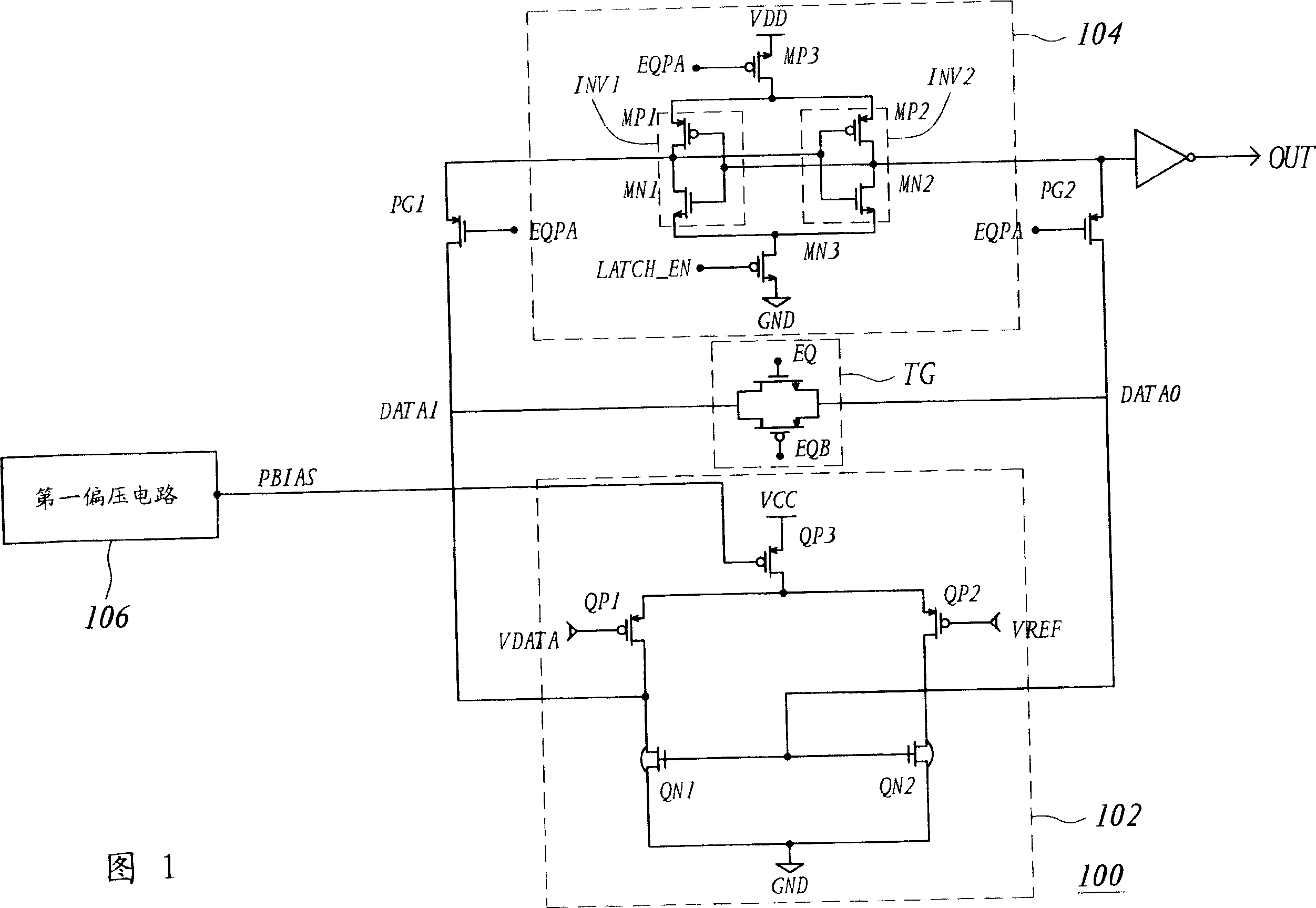
[0031] Please refer to FIG. 1 , which shows a circuit diagram of a sense amplifier 100 according to a first embodiment of the present invention. The sense amplifier 100 includes a first-stage amplifier 102 , a second-stage amplifier 104 and a first bias circuit 106 , the first-stage amplifier 102 includes an amplifier circuit, and the second-stage amplifier 104 includes a latch. The amplifier circuit is used for receiving the data voltage VDATA and the reference voltage VREF. According to the data voltage VDATA and the reference voltage VREF, the amplifier circuit outputs the first data output DATA1 and the second data output DATA0 respectively, and is received by the second stage amplifier 104 . Furthermore, the amplifier circuit is preferably a differential amplifier circuit or an operational conduction amplifier circuit.

[0032] The first-stage amplifier 102 includes three MOS transistors, such as a first PMOS transistor QP1 , a second PMOS transistor QP2 and a third PMOS...

no. 2 example

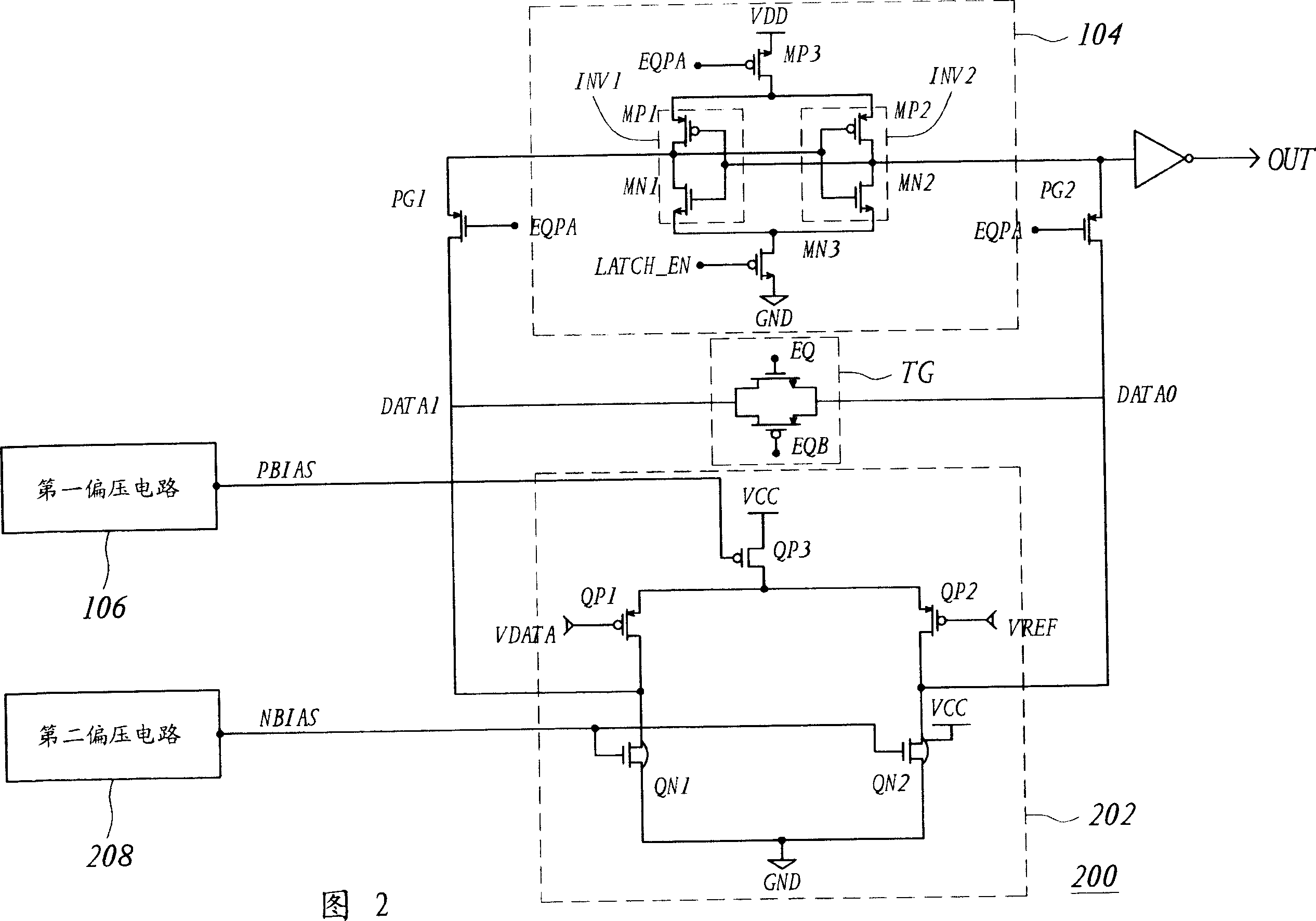
[0045] Please refer to FIG. 2 , which shows a circuit diagram of a sense amplifier according to a second embodiment of the present invention. The sense amplifier 200 includes a first-stage amplifier 202 and a second-stage amplifier 204 , and further includes a second bias circuit 208 which is different from the first embodiment. The gates of the fourth MOS transistor QN1 and the fifth MOS transistor QN2 are replaced to receive the adjustment voltage NBIAS generated by the second bias circuit 208 instead of being coupled to the drain of the second PMOS transistor QP2 as shown in FIG. 1 . The fourth MOS transistor QN1 and the fifth MOS transistor QN2 are used for loading of the first stage amplifier 202 .

[0046] In summary, the sense amplifier according to the present invention has the following advantages:

[0047] 1. Reduce power consumption and increase operating speed

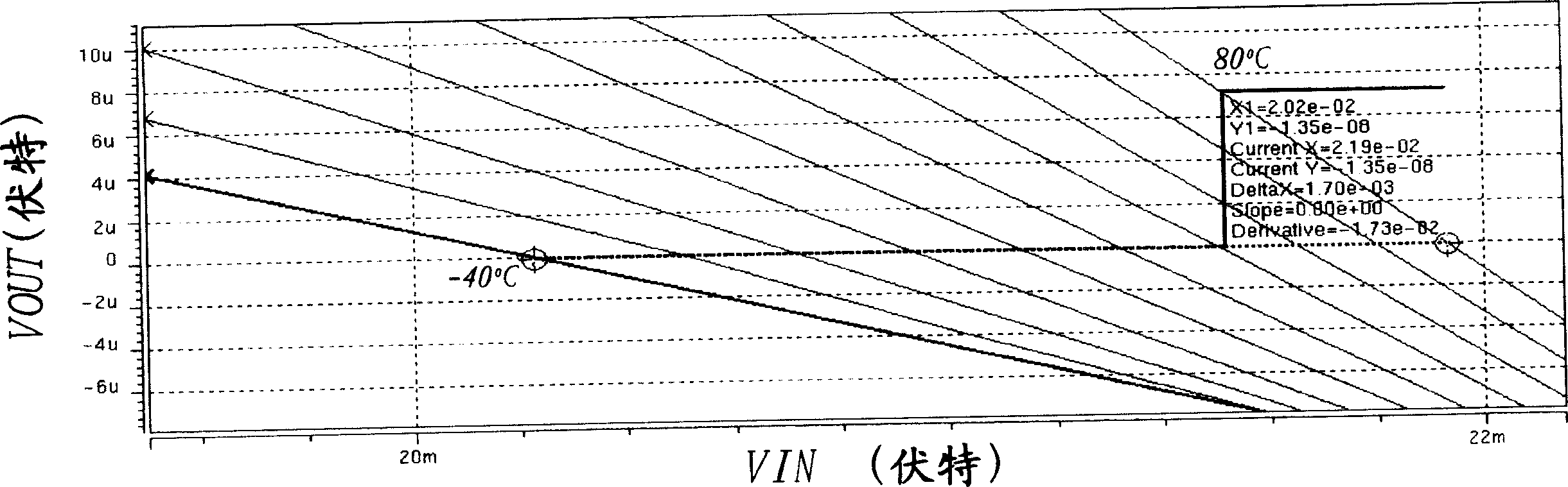
[0048] When the latch requires a higher bias voltage (external voltage) to operate, such as Figure ...


PUM


Abstract

A sense amplifier, including a first stage amplifier and a second stage amplifier, for compensating input offset voltage changes due to temperature variation of the sense amplifier. The first stage amplifier receives a data voltage and a reference voltage, and outputs a first data output and a second data output. The first stage amplifier receives an adjusted voltage, and is biased at an internal voltage. The second stage amplifier includes a latch, for level-shifting and amplifying the first and second data output, and is biased at an external voltage. The sense amplifier further includes a bias circuit, for generating the adjusted voltage according to temperature variation of the sense amplifier, to reduce the input offset voltage changes.

Description

technical field [0001] The present invention relates to a sense amplifier, and more particularly to a sense amplifier having an amplifier stage and a latch stage capable of compensating input offset. Background technique [0002] With the high development of modern digital systems and the demand for multitasking functions, it is inevitable that semiconductor memory components with larger memory capacity and higher data access speed are required to meet the needs. [0003] In order to achieve a higher data access speed, one solution is to increase the speed at which the sense amplifier senses and amplifies the data read from the memory cell. The sense amplifier usually includes several differential amplifiers, wherein the voltage difference between the tiny voltage sensed from the data of the memory unit and the corresponding reference voltage is amplified to output a proportional voltage. [0004] However, when reducing the data voltage sensed by the sense amplifier in orde...

Claims


Application Information

Patent Timeline
Patent Type & Authority Applications(China)
IPC IPC(8): G11C7/06
CPCG11C7/065G11C7/04G11C7/08
Inventor 陈重光
Owner MACRONIX INT CO LTD
Why Eureka
Try Eureka