Semiconductor package with contact support layer and method to produce the package

A technology of semiconductors and semiconductor tubes, applied in semiconductor/solid-state device manufacturing, semiconductor devices, semiconductor/solid-state device components, etc., can solve problems such as unreliability and complicated methods, and achieve reliable support, simple and fast methods, and support layers Simple and Flexible Effects

Inactive Publication Date: 2007-02-14
INFINEON TECH AG
View PDF1 Cites 2 Cited by
  • Summary
  • Abstract
  • Description
  • Claims
  • Application Information

AI Technical Summary

Problems solved by technology

The method is complex and unreliable

Method used


Image

  • Semiconductor package with contact support layer and method to produce the package
  • Semiconductor package with contact support layer and method to produce the package
  • Semiconductor package with contact support layer and method to produce the package

Examples


Embodiment Construction

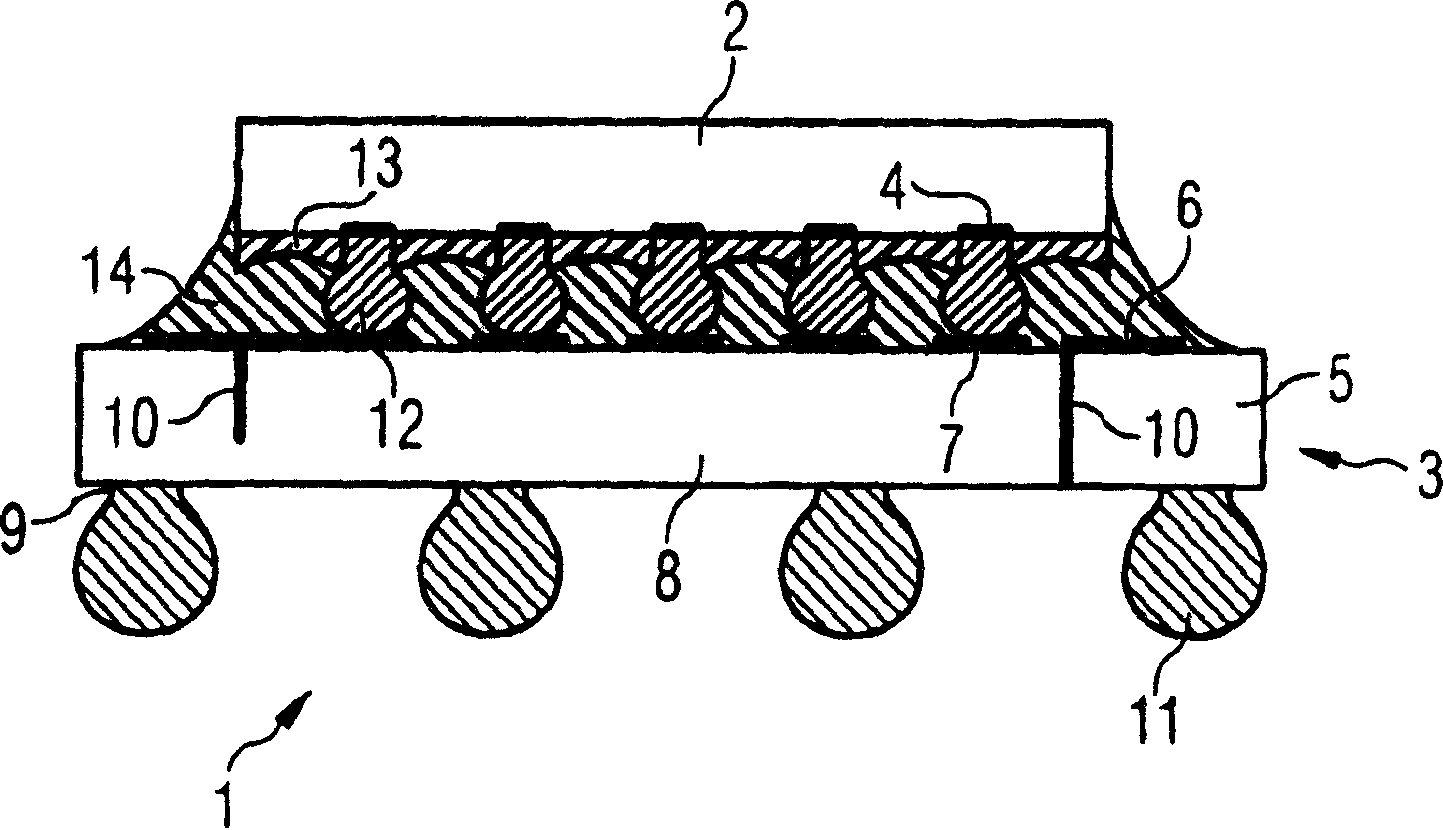
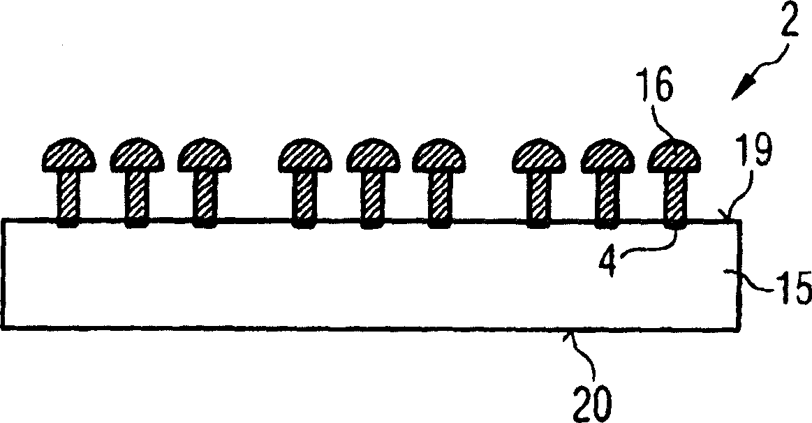
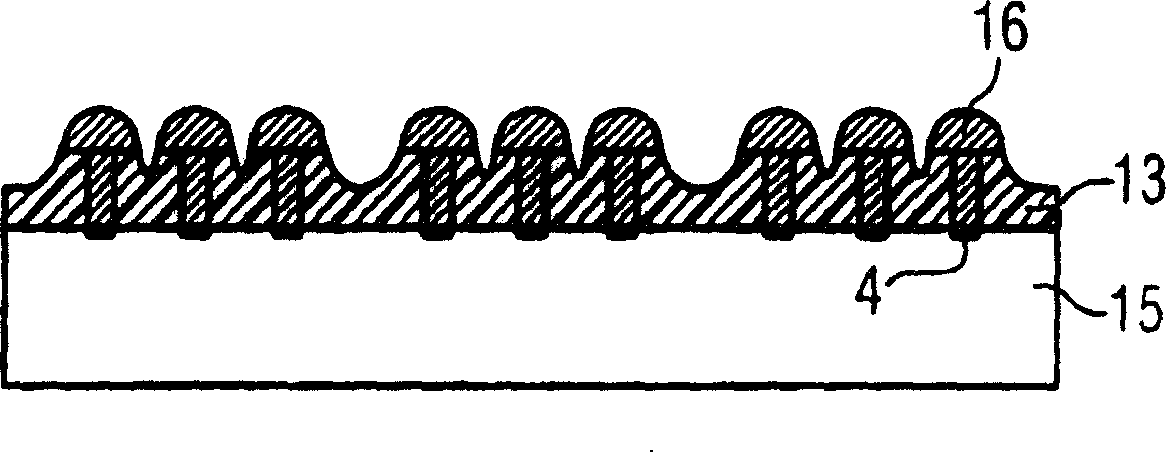
[0036] figure 1 Shown is a cross-sectional view of a semiconductor package 1 comprising a semiconductor die 2 mounted to a redistribution plate 3 by flip-chip technology.

[0037] Semiconductor die 2 includes an active surface including a plurality of die contact pads 4 and a passive surface. The redistribution plate 3 comprises a sheet of non-conductive core material 5 and includes a plurality of upper conductive traces 6 and upper contact pads 7 on its upper surface and a plurality of lower conductive traces 8 and external contacts on its bottom surface. District 9. The redistribution plate 3 also includes a plurality of substantially vertical conductive vias 10 electrically connecting the upper contact pads 7 with the contact areas 9 on the bottom surface of the redistribution plate 3 . Solder balls 11 are attached to the external contact areas 9 to provide an electrical connection from the package 1 to an external circuit board (which is not shown in the figure).

[003...


PUM


Abstract

A semiconductor package comprises a substrate which includes a plurality of conducting traces and upper contact areas on its upper surface and a second plurality of lower conductive traces and external contact areas on its bottom surface and external conducting means attached to the external contact areas. The semiconductor package also includes a semiconductor die comprising an active surface with a plurality of die contact pads, electrically connected to the contact areas of the substrate by conducting means. A support layer between the conducting means on the active surface of the die covers at least the base portion of the conducting means.

Description

technical field [0001] The invention relates to a method of manufacturing a semiconductor package comprising a contact support layer. Background technique [0002] DE 101 33 791 A1 discloses a method for arranging and attaching preformed solder balls to a semiconductor chip. This method is complex and unreliable. Contents of the invention [0003] It is an object of the present invention to produce a more reliable semiconductor package and a simple and cost-effective method for producing the package. [0004] This object of the invention is solved by the subject-matter of the independent claims. Further improvements emerge from the subject-matter of the dependent claims. [0005] A method of assembling a semiconductor package comprising a contact support layer according to the invention comprises the following steps. A semiconductor wafer including a plurality of semiconductor dies or chips is provided. Each semiconductor die includes an active surface having a plural...

Claims


Application Information

Patent Timeline
Patent Type & Authority Applications(China)
IPC IPC(8): H01L21/60H01L23/485H01L21/68H01L21/56H01L23/31
CPCH01L2924/01015H01L24/12H01L2924/01082H01L2221/68327H01L2224/11003H01L24/94H01L21/563H01L2924/01322H01L2924/15311H01L2224/13099H01L24/11H01L2924/01013H01L2924/014H01L2224/11822H01L2224/32225H01L21/6836H01L2224/274H01L24/27H01L2224/73204H01L24/16H01L21/6835H01L2924/01005H01L2924/01033H01L2924/01006H01L2924/01078H01L2224/16225H01L23/3157H01L2224/05571H01L2224/05573H01L2924/00014H01L2224/81011H01L2924/00H01L2224/05599
Inventor K·陈G·奥夫纳李维民
Owner INFINEON TECH AG
Why Eureka
Try Eureka