Semiconductor memory cell array having mos transistors and method for forming the same

A storage unit and semiconductor technology, applied in semiconductor/solid-state device manufacturing, transistors, semiconductor devices, etc., can solve the problems of reducing coverage tolerance and inability to guarantee layer coverage accuracy, so as to reduce the standard distance, improve unit performance, and low The effect of contact resistance

Inactive Publication Date: 2007-02-21
QIMONDA
View PDF0 Cites 6 Cited by
  • Summary
  • Abstract
  • Description
  • Claims
  • Application Information

AI Technical Summary

Problems solved by technology

However, improved lithographic setups to reduce the coverage tolerance of the gate layer of select transistors relative to the trench capacitor layer cannot guarantee sufficient layer coverage accuracy starting with 65nm technology formation

Method used


Image

  • Semiconductor memory cell array having mos transistors and method for forming the same
  • Semiconductor memory cell array having mos transistors and method for forming the same
  • Semiconductor memory cell array having mos transistors and method for forming the same

Examples


Embodiment Construction

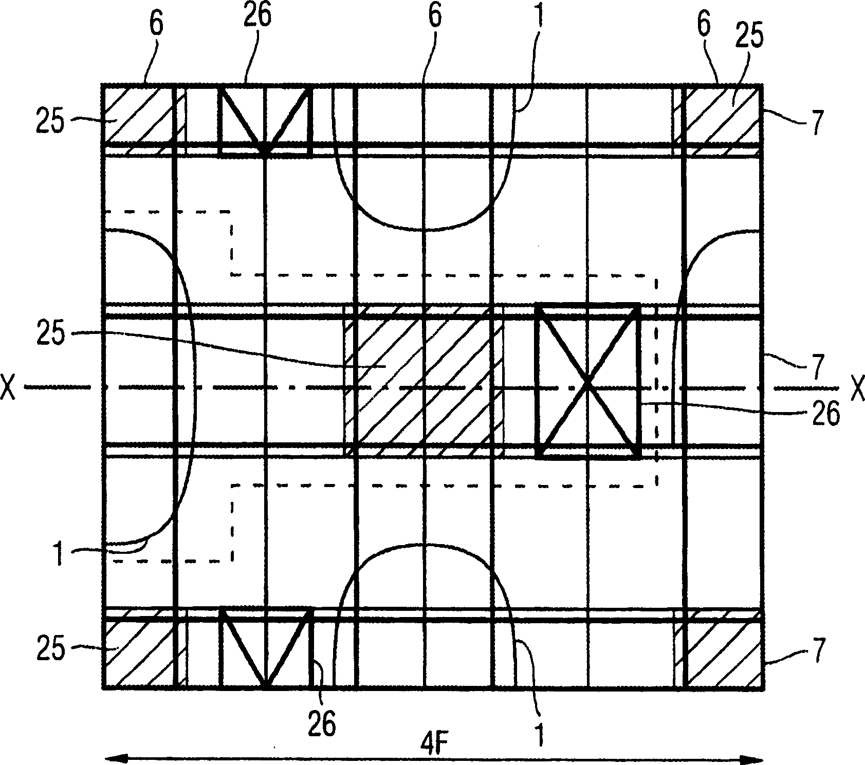
[0029]The invention is illustrated by the process of forming a silicon-based DRAM. The individual structures of the dynamic memory cells are preferably formed by means of silicon planar technology, which comprises a series of individual processes carried out in each case in a full-area manner on the surface of the silicon substrate, where the Local changes. In DRAM memory fabrication, multiple memory cells are formed simultaneously.

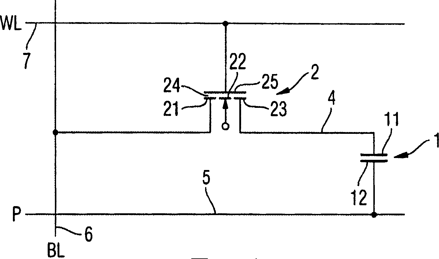
[0030] In DRAM, the application is mainly composed of a single-transistor memory cell, and its circuit diagram is as follows figure 1 shown. A one-transistor memory cell includes a storage capacitor 1 and a selection transistor 2 . The selection transistor 2 is preferably formed as a field effect transistor having a first source / drain electrode 21 , a second source / drain electrode 23 and an active region 22 therebetween. The gate insulating layer 24 and the gate 25 are positioned on the top of the active region 22, acting like a flat plate ca...


PUM


Abstract

In a semiconductor memory including an array of memory cells, each memory cell includes a trench capacitor, the trench capacitor including an inner electrode, an outer electrode and a dielectric layer disposed between the inner electrode and the outer electrode, and a selection transistor, the selection transistor including a first source / drain area, a second source / drain area and a channel region disposed between the first source / drain area and the second source / drain area in a recess, the trench capacitor and the selection transistor of each memory cell are disposed side by side, the first source / drain area of the selection transistor being electrically connected to the inner electrode of the trench capacitor, the recess in which the channel region of the selection transistor is formed being located self aligned between the trench capacitor of the memory cell and the trench capacitor of an adjacent memory cell.

Description

technical field [0001] The present invention relates to a semiconductor memory including a memory cell array and a manufacturing method thereof, and more particularly, to a semiconductor memory including a memory cell array and a manufacturing method thereof, wherein each memory cell includes a trench capacitor and a Select transistors with recessed gates. Background technique [0002] In dynamic random access memory (DRAM), the application is mainly implemented by a single-transistor memory cell consisting of a select transistor and a storage capacitor, where information is stored in the form of electric charges. DRAM includes an array of memory cells connected in rows and columns. Typically, rows are designated as word lines and column lines are designated as bit lines. The selection transistor and the storage capacitor of the memory cell are connected to each other in such a manner that when the selection transistor is driven through the word line, the charge of the sto...

Claims


Application Information

Patent Timeline
Patent Type & Authority Applications(China)
IPC IPC(8): H01L27/108H01L21/8242
CPCH01L27/10876H01L27/10861H10B12/038H10B12/053
Inventor G·恩德尔斯M·施特拉泽P·福伊格特B·菲舍尔
Owner QIMONDA
Why Eureka
Try Eureka