Method of forming circuit pattern on printed circuit board

A printed circuit board, circuit pattern technology, applied in the direction of printed circuit, printed circuit, printed circuit manufacturing, etc., can solve problems such as short circuit, error, non-uniformity, etc.

Inactive Publication Date: 2007-03-07
SAMSUNG ELECTRO MECHANICS CO LTD
View PDF0 Cites 15 Cited by
  • Summary
  • Abstract
  • Description
  • Claims
  • Application Information

AI Technical Summary

Problems solved by technology

However, since inkjet printing is used, the wiring pattern forming process must be performed several times to obtain a circuit pattern of a desired thickness, and during the process, there is a risk of errors such as unevenness and short circuits.

Method used


Image

  • Method of forming circuit pattern on printed circuit board
  • Method of forming circuit pattern on printed circuit board
  • Method of forming circuit pattern on printed circuit board

Examples


Embodiment Construction

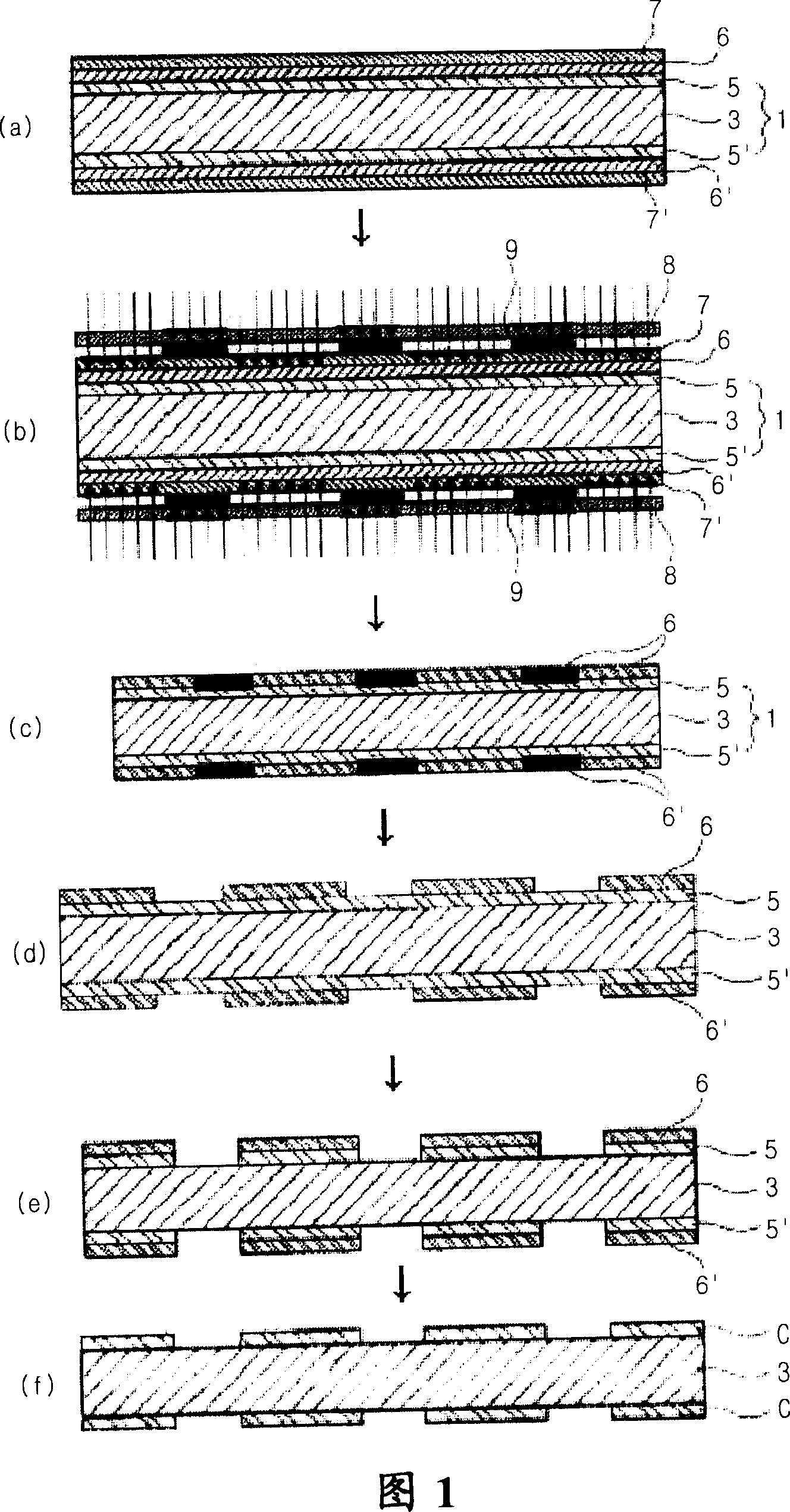
[0030] Hereinafter, embodiments of the present invention will be described in more detail with reference to the accompanying drawings. In the description with reference to the drawings, those same or corresponding components are given the same reference numerals regardless of whether the figure numbers are the same, and redundant explanations are omitted.

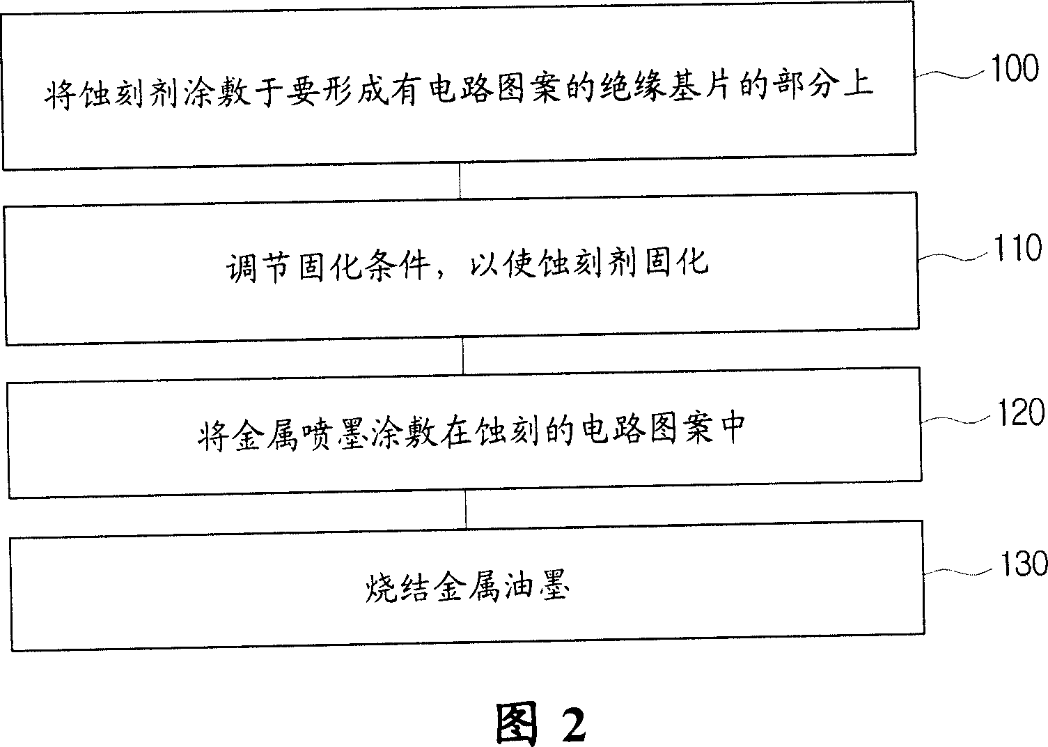
[0031] FIG. 2 shows a flowchart of a process of forming a circuit pattern on a printed circuit board according to an embodiment of the present invention.

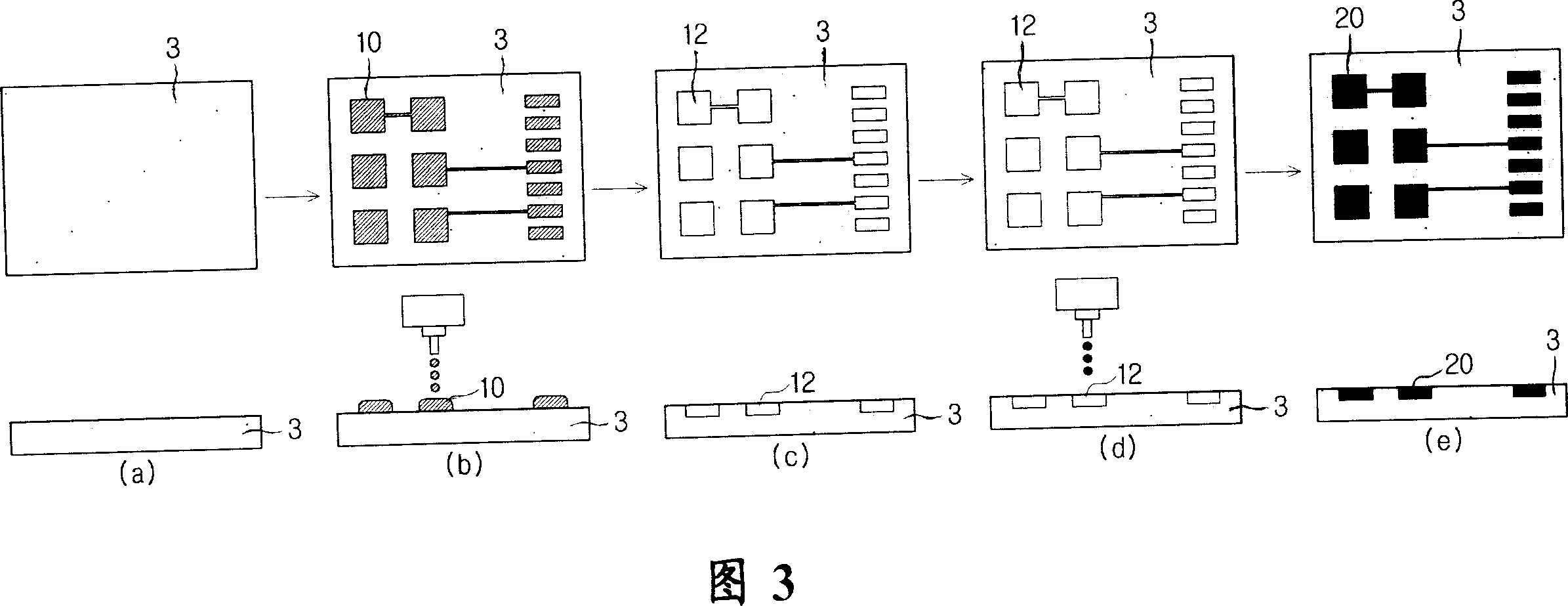
[0032] The present invention is characterized by a method of forming a circuit pattern on a printed circuit board, wherein processes such as plating, exposure, and etching (typically time-consuming and expensive circuit patterning processes) are eliminated, and by The printing method sprays etchant and metal ink to form circuit patterns to provide fine patterns and realize pattern width adjustment.

[0033] To this end, an etchant is first applied (100) on a portion of ...


PUM


Abstract

The invention discloses a method for forming a circuit pattern on a printed circuit board. The method for forming a circuit pattern on a printed circuit board includes: (a) applying an etchant to an insulating substrate portion where a circuit pattern is to be formed; (b) curing the etchant by adjusting curing conditions; (c) applying a metal ink On the etched circuit pattern; and (d) sintering metal ink, since the process of coating photoresist (PR), exposure and development can be removed to simplify the whole process, the manufacturing cost is greatly reduced, and it can be achieved by spending a small amount of process And time precisely form the circuit pattern of the printed circuit board.

Description

[0001] Cross References to Related Applications [0002] This application claims priority from Korean Patent Application No. 2005-0081578 filed with the Korean Intellectual Property Office on September 2, 2005, the entire contents of which are hereby incorporated by reference. technical field [0003] The present invention relates to a method for forming a circuit pattern, and more particularly, to a method for forming a circuit pattern on a printed circuit board. Background technique [0004] Generally, a circuit pattern of a printed circuit board is formed by performing processes such as copper plating, photoresist coating, exposure, development, and etching on an insulating substrate. Meanwhile, as the recent electronic products tend to be small in size and have more functions, chip components are required to have both small size and more functions and low cost. Thus, technical improvements in the process of forming circuit patterns on printed circuit boards are required...

Claims


Application Information

Patent Timeline
Patent Type & Authority Applications(China)
IPC IPC(8): H05K3/06H05K3/00H05K1/16
CPCH05K2203/013H05K3/1258H05K3/107H05K1/0346H05K3/125H05K2201/09036H05K3/002H05K2201/0154H05K3/1208H05K3/06
Inventor 金永财郑在祐刘永锡
Owner SAMSUNG ELECTRO MECHANICS CO LTD
Why Eureka
Try Eureka