
Machine vision based LCD spot flaw detection method and system

A liquid crystal display, machine vision technology, applied in optical testing flaws/defects, instruments, image data processing, etc., can solve problems such as difficulty in automatic detection of spot defects

Inactive Publication Date: 2007-03-14
HARBIN INST OF TECH +1
View PDF0 Cites 19 Cited by
  • Summary
  • Abstract
  • Description
  • Claims
  • Application Information

AI Technical Summary

Problems solved by technology

In addition, there is no uniform definition and detection standard for spot defects in the entire LCD industry, which brings difficulties to the automatic detection of spot defects

Method used


Image

  • Machine vision based LCD spot flaw detection method and system
  • Machine vision based LCD spot flaw detection method and system
  • Machine vision based LCD spot flaw detection method and system

Examples


Embodiment Construction

[0025] The technical solution of the present invention will be further described below in conjunction with the accompanying drawings.

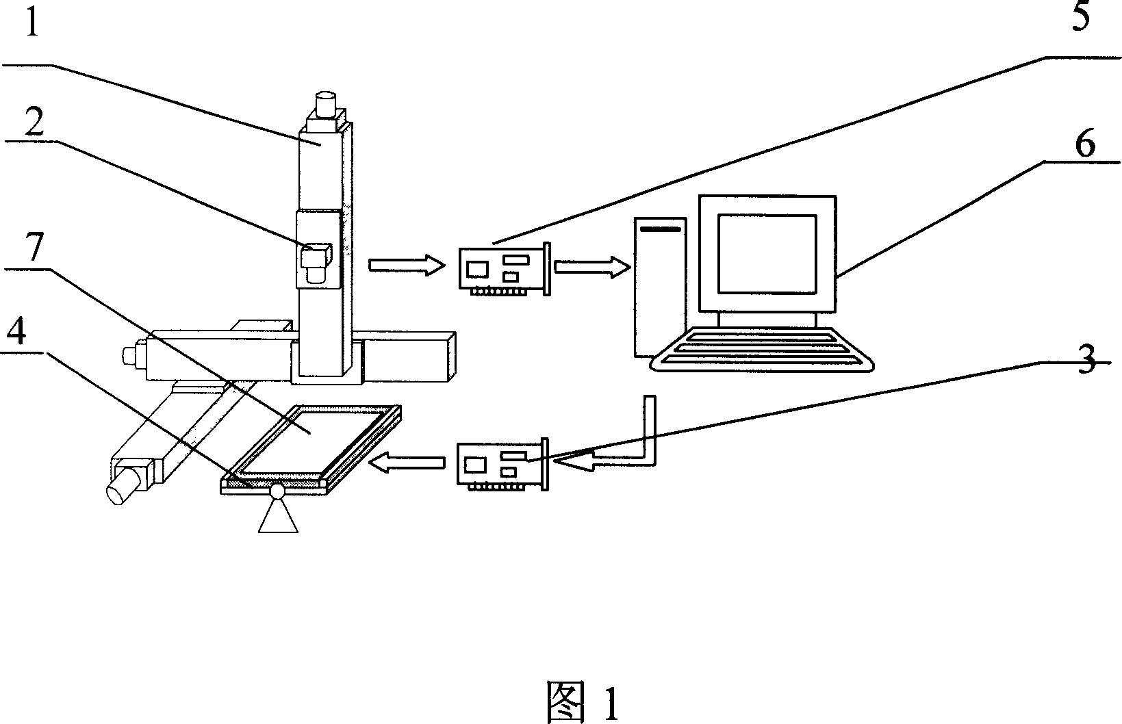
[0026] Referring to FIG. 1 , the liquid crystal display defect detection system in this specific embodiment is composed of a CCD camera 2 , an image acquisition card 5 , a computer 6 , a three-axis precision positioning platform 1 , a liquid crystal display drive module 3 and an object stage 4 . The stage 4 is fixedly connected to the three-axis precision positioning platform 1, and is connected to the interface of the dedicated display driver module 3 through a cable. On the stage 4, the CCD camera 2 is fixed on the three-axis precision positioning platform 1 as an image acquisition device, so that it can move to a corresponding position under the control of the computer 6 according to the model of the liquid crystal display 7 to be tested for image acquisition.

[0027] The image acquisition card 5 is a standard analog or digital image acqui...


PUM


Abstract

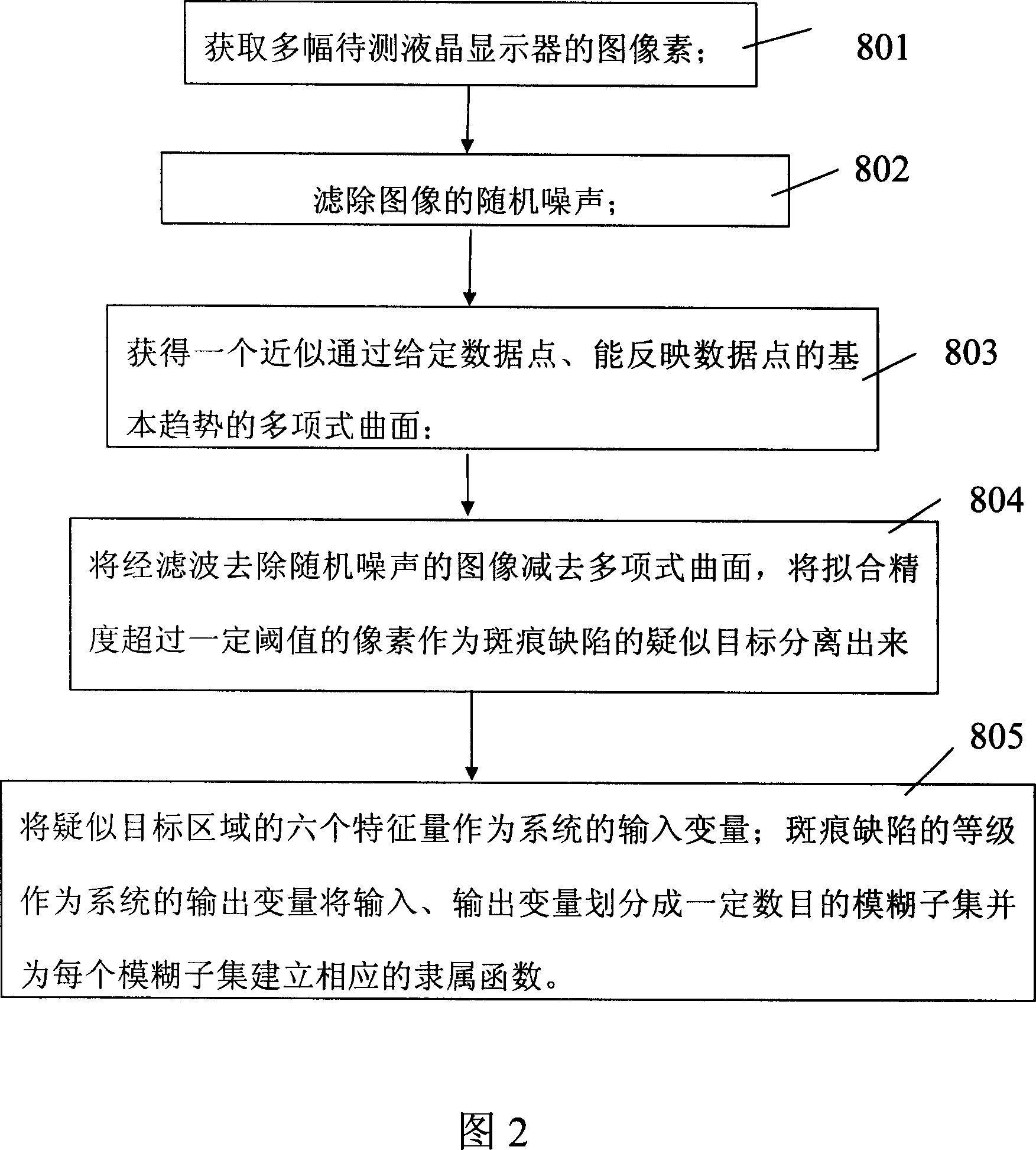
The disclosed detect method for LED display stain based on machine vision comprises: acquiring some images of target display to filter noise and one polynomial curves that can show the data trend; subtracting the image by the polynomial curve to separate the pixel over threshold as the suspected stain target; selecting the contrast grade, area, edge parameter, position, gray scale evenness, and shape of the suspected target as input variables; selecting stain defect grade as output variable; dividing the input and output variables into some fuzzy subsets with membership grade function.

Description

technical field [0001] The invention relates to a spot defect detection system of a liquid crystal display, in particular to a machine vision-based spot defect detection system. Background technique [0002] The production process of liquid crystal displays is very complicated, and although most of the processes are completed in a clean room, some visual defects will inevitably appear. There are many types of visual defects in liquid crystal displays, which can generally be divided into three categories according to the area and shape of the defects: point defects, line defects and surface defects. Among them, surface defects can be divided into two types: block defects and spot defects (called mura in English, which comes from Japanese, meaning dirt and spots, and is the most common surface defect). Point defects, line defects, and block defects are mainly caused by electrical causes such as short circuits, open circuits, and bad transistors in thin-film transistor (TFT) a...

Claims


Application Information

Patent Timeline
Patent Type & Authority Applications(China)
IPC IPC(8): G01N21/88G06T1/00G06F17/00
Inventor 张健张昱吴丽莹刘泊晗
Owner HARBIN INST OF TECH
Learn More