
LCD driving mechanism for thin film transistor

A liquid crystal display and thin film transistor technology, which is applied in the field of thin film transistor liquid crystal display driving devices, can solve problems such as increasing the power consumption of modules, and achieve the effects of reducing power consumption and avoiding waste of dynamic current.

Inactive Publication Date: 2007-03-14
CHUNGHWA PICTURE TUBES LTD
View PDF0 Cites 6 Cited by
  • Summary
  • Abstract
  • Description
  • Claims
  • Application Information

AI Technical Summary

Problems solved by technology

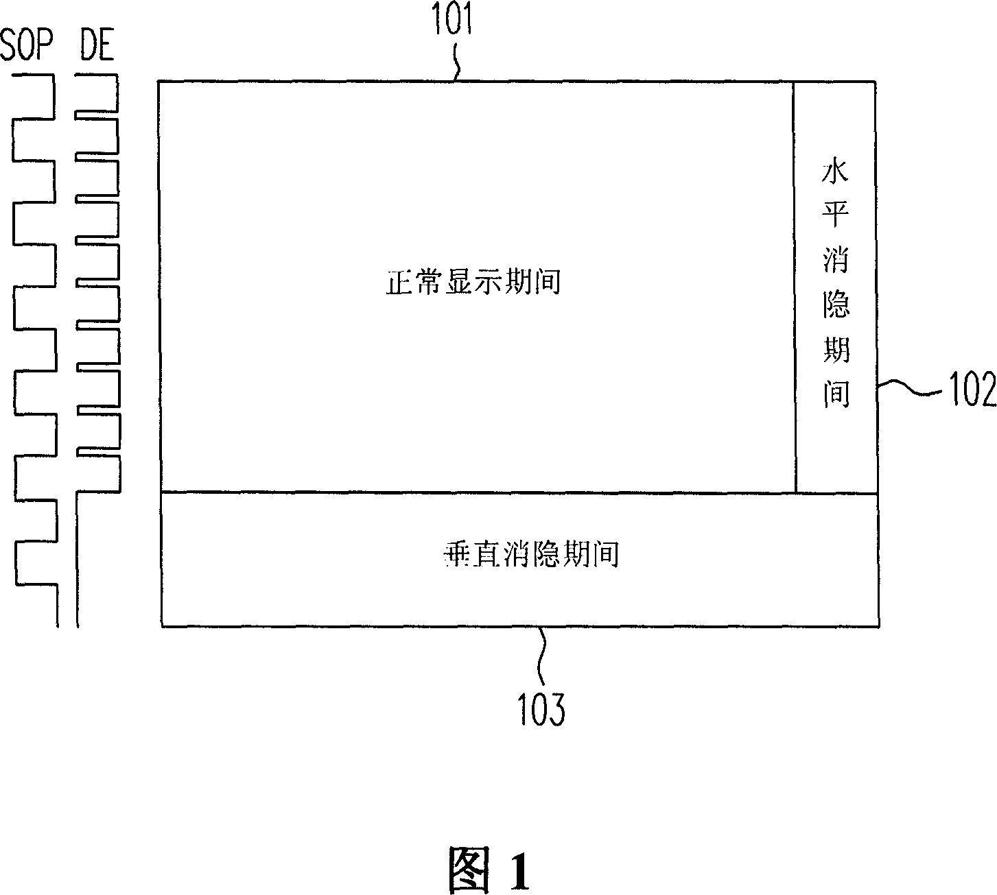
[0003] It can be seen from FIG. 1 that although the vertical blanking period 103 is a blank time when no image is displayed, the current source drive circuit continues to output the signal SOP with alternating positive and negative polarities during this period. That is to say, the source drive circuit is still consuming current, which virtually increases the power consumption of the module

Method used


Image

  • LCD driving mechanism for thin film transistor
  • LCD driving mechanism for thin film transistor
  • LCD driving mechanism for thin film transistor

Examples


Embodiment Construction

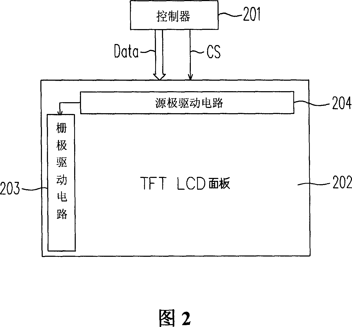
[0039] A thin film transistor liquid crystal display driving device according to an embodiment of the present invention will be described below. Please refer to FIG. 2 first. FIG. 2 is a driving circuit of the liquid crystal display of this embodiment, including a controller 201 , a source driving circuit 204 , and a gate driving circuit 203 .

[0040] In this embodiment, the controller 201 is an application-specific integrated-circuit (ASIC), responsible for outputting the pixel data Data and the control signal CS to the source driving circuit 204 . The control signal CS is a collection of multiple signals, including a start pulse signal (start pulse) and a latch pulse signal (latch pulse), etc. These signals will be described in more detail later.

[0041] The source drive circuit 204 has a plurality of output terminals, and its main function is to convert the pixel data Data from a digital signal to an analog data level according to the latch pulse signal, and then output i...


PUM


Abstract

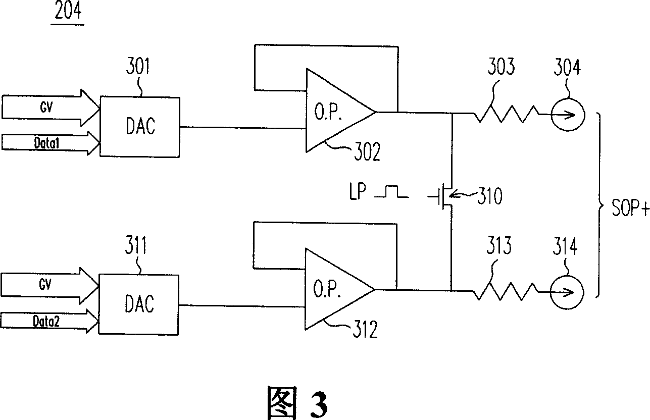
The TFT LCD driver comprises a controller to output latch pulse signal and a grid drive circuit with multiple output ports to output data level according to pulse signal and some switch devices arranged between two near output ports to conduct ports during the vertical blanking period. This invention can prevent the consumption of grid drive circuit without effect to figure quality.

Description

technical field [0001] The invention relates to a driving device of a thin film transistor liquid crystal display, and in particular to a driving device of a thin film transistor liquid crystal display capable of reducing power consumption. Background technique [0002] As shown in FIG. 1 , the current driving method of thin-film transistor (TFT for short) liquid crystal display (LCD for short) is in order to be compatible with the traditional cathode ray tube (cathode-ray tube, CRT for short). ) display common control signal, within a frame field (frame field), in addition to the normal display period 101 with images, it also includes a horizontal blanking period (horizontal blanking time) 102 and vertical blanking Period (vertical blanking time) 103 . In FIG. 1 , DE represents a data drive signal (dataenable), and SOP represents an output signal of a source driver IC (where IC is an integrated-circuit, which is an abbreviation for an integrated circuit). [0003] It can ...

Claims


Application Information

Patent Timeline
IPC IPC(8): G09G3/36G09G3/20G02F1/133
Inventor 简志荣
Owner CHUNGHWA PICTURE TUBES LTD
Learn More