Method and device for cleaning semiconductor crystal wafer

A technology for cleaning equipment and wafers, applied in liquid cleaning methods, cleaning methods and utensils, semiconductor/solid-state device manufacturing, etc., can solve the problem of limited wafer pre-rinsing capabilities, unsuitable operating habits, and large consumption of pure water and other problems, to achieve the effect of saving pure water consumption, saving pure water consumption, and avoiding water pollution

Active Publication Date: 2007-04-04
WUXI CHINA RESOURCES HUAJING MICROELECTRONICS
View PDF0 Cites 3 Cited by
  • Summary
  • Abstract
  • Description
  • Claims
  • Application Information

AI Technical Summary

Problems solved by technology

The problems in the structure and cleaning method of this kind of flushing tank are: 1. The discs taken out from the corrosion tank must cross the top of the overflow tank to reach the pre-flushing tank after pre-flushing, and there is acid water dripping in the tank during the process. Possibly, there is a hidden danger of polluting the flushing tank; if this situation is to be avoided, the operator must deliberately bypass the top of the overflow tank, which does not conform to operating habits and brings inconvenience to actual work
2. The four water tanks are close together and have the same height. When more than two batches of discs are flushed at the same time, the overflowing water can easily overflow into the adjacent water tanks and cause mutual pollution.
3. Each flushing tank uses a separate water inlet pipe, and the amount of pure water is relatively large
4. The original pre-rinse tank enters water from the bottom and drains water through small holes at the bottom and overflow at the top, so the pre-rinse capacity for wafers is limited

Method used


Image

  • Method and device for cleaning semiconductor crystal wafer
  • Method and device for cleaning semiconductor crystal wafer
  • Method and device for cleaning semiconductor crystal wafer

Examples


Embodiment 1

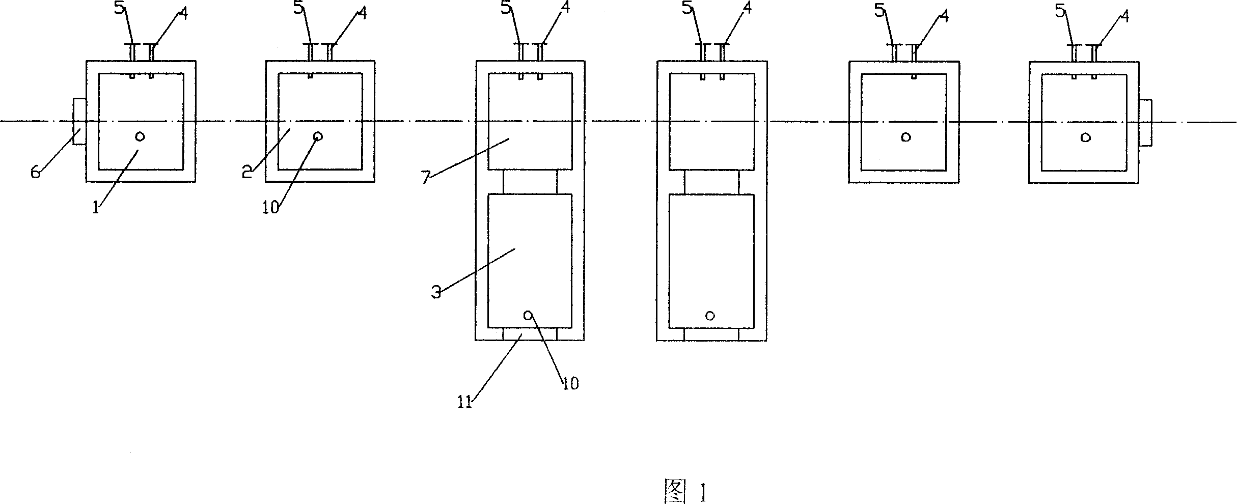
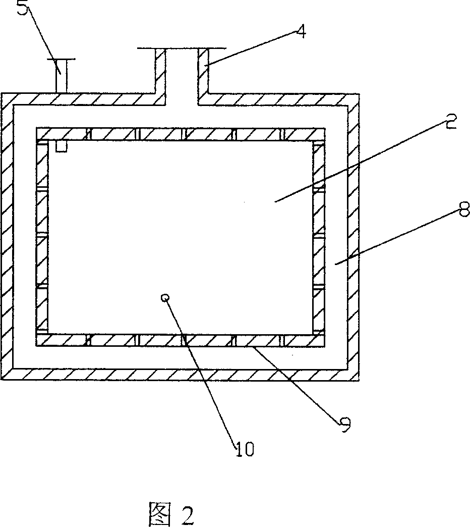
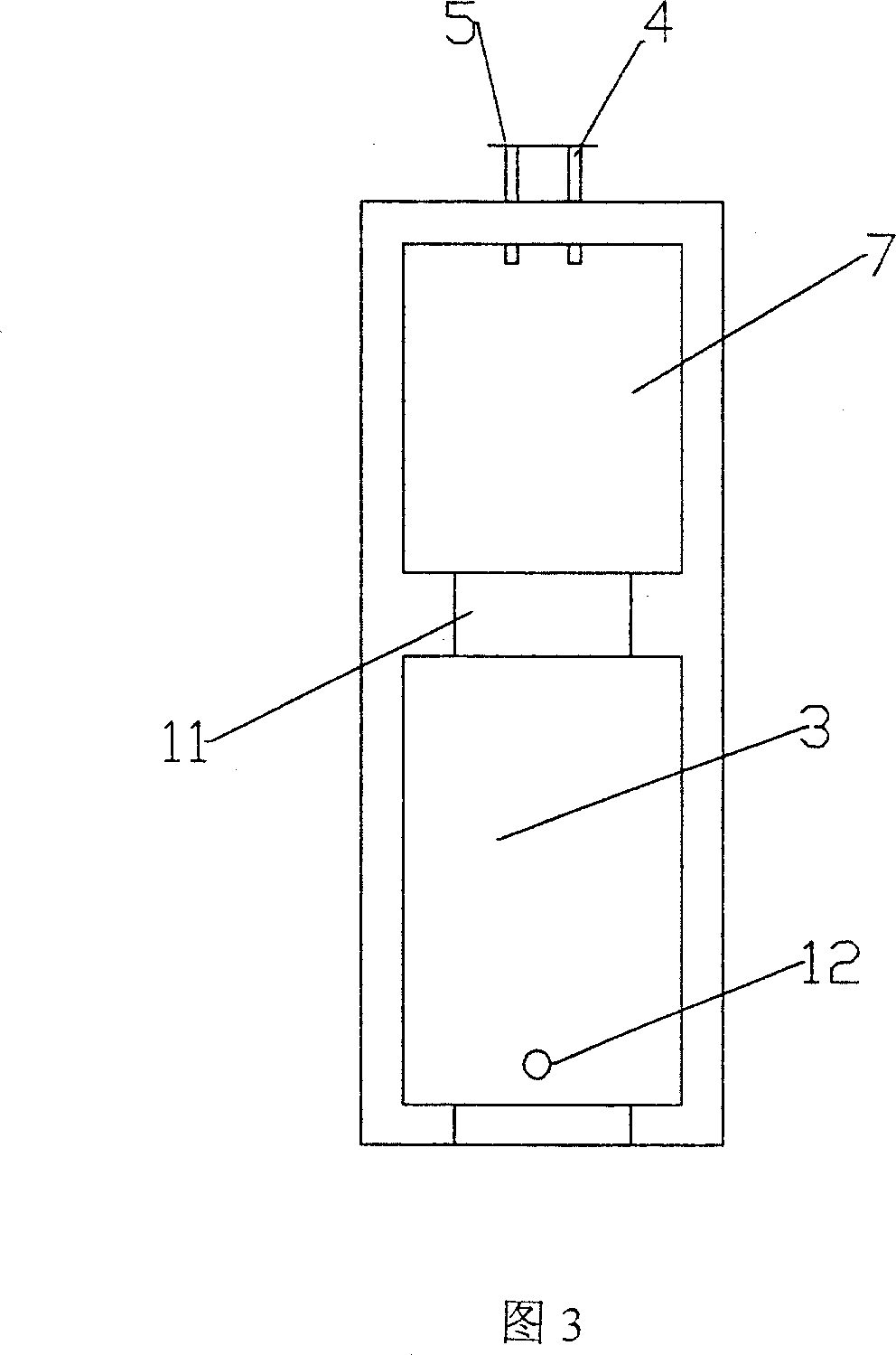
[0024] The present invention mainly adopts corrosion tank 1, spray type pre-flushing tank 2, step type high and low flushing tank 7, 3 two to form a group (system) to be the left step type flushing tank, independent of each other. When in use, two sets of left and right stepped flushing tanks can be used at the same time. There is a space between the left stepped flushing tank and the right stepped flushing tank (corrosion tank, spray pre-flushing tank, stepped high and low flushing tank), which can prevent the overflowing water from the tank from polluting each other. Ladder-type high and low flushing tanks 7 and 3 are arranged in front and back in steps, corrosion tank 1, spray pre-flushing tank 2, and stepped high and low flushing tank 3 are respectively connected to water inlet pipe 4 and air intake pipe 5 at the top and back, and elevator 6 is equipped on corrosion tank 1 , the elevator 6 continuously lifts the semiconductor wafer during operation. The intake pipe 5 is a...

Embodiment 2

[0034] In the embodiment of the present invention, two groups of the same left and right stepped flushing tanks in the first embodiment are used simultaneously. The process parameters are as follows: the liquid temperature of the etching tank is 30°C; 10 seconds before the completion of the corrosion operation, turn on the pure water, stepped flushing tank, and nitrogen switch of the spray pre-rinsing tank; put the semiconductor wafer into the spray pre-rinsing tank. Lift and pull up and down in the flushing tank 5 times for 10 seconds; then put the semiconductor wafer into the stepped low-flush water tank and flush for 4 minutes; transfer the semiconductor wafer to the stepped high-flush water tank and continue flushing for 4 minutes minutes, finally take it out, and dry it for 5 minutes at a speed of 880 rpm in a centrifugal dryer.

Embodiment 3

[0035] Embodiment 3: In the embodiment of the present invention, two groups of the same left and right stepped flushing tanks as in Embodiments 1 and 2 are used at the same time. The process parameters are as follows: the temperature of the liquid in the corrosion tank is 32°C; 12 seconds before the completion of the corrosion operation, turn on the pure water in the spray pre-rinse tank, the step-type flushing tank, and the nitrogen switch; put the semiconductor wafer into the spray pre-rinse tank. Pull up and down 6 times in the flushing tank for 12 seconds; then put the semiconductor wafer into the stepped low-flush water tank for 5 minutes; transfer the semiconductor wafer to the stepped high-flush water tank and continue flushing for 5 minutes minutes, finally take it out, and dry it for 6 minutes at a speed of 920 rpm in a centrifugal dryer.

[0036] In the second and third embodiments of the present invention, the semiconductor wafers cleaned by the above process parame...


PUM


Abstract

A cleaning method and equipment of semiconductor wafer belongs to the equipment of wet-etching working procedure. The one group of equipment (system) relates to cankerous canal, spray advance washing canal, and stepped high and low rushing canal for the wet-etching, removing glue and cleaning in the process of semiconductor wafer production. Water from one hose cleans two groups of wafer at same time to keep the cleaning of the wafer surface. It reduces the hidden trouble of safety to working procedure and avoids the pollution of water and mark of acid. It changes the influent fashion of primary advance washing canal from bottom to brim of spray one and the water spout into the canal through the hole of the brim. It adds the spouting pressure in concentrated direction and cleans the wafer drastically to improve the wet-etching's rushing effort. The stepped high and low rushing canal is a whole, and water enters from the high end to the low end from top and bottom and saves half of water.

Description

technical field [0001] The present invention relates to a semiconductor wafer cleaning method and its cleaning equipment, specifically for flushing in processes such as wet etching, degumming, and cleaning in the production process of semiconductor wafers, and belongs to the wet etching process device of. Background technique [0002] At present, the four flushing tanks used for wet etching, degumming, cleaning and other processes in the semiconductor wafer production process are lined up and close together, from etching tank → pre-rinsing tank → two overflow tanks The troughs form a group, and the left and right groups can also be used, and a lift is installed on the corrosion tank. Each flushing tank uses a separate water inlet pipe (rear), and the N2 (nitrogen) pipe is connected to the back of the overflow tank to protect the wafers by bubbling during flushing and cleaning. The etched wafers are pre-rinsed before being further rinsed in either of the overflow tanks. Th...

Claims


Application Information

Patent Timeline
Patent Type & Authority Applications(China)
IPC IPC(8): H01L21/302H01L21/306B08B3/00
Inventor 潘之炜王荣华万辉
Owner WUXI CHINA RESOURCES HUAJING MICROELECTRONICS
Why Eureka
Try Eureka