Method of manufacturing a non-volatile memory device

A non-volatile storage and device technology, applied in the fields of electric solid-state devices, semiconductor devices, semiconductor/solid-state device manufacturing, etc., can solve problems such as damage to the programming characteristics of flash memory devices, improve data erasure characteristics, prevent thickness changes, Improve the effectiveness of data programming features

Inactive Publication Date: 2007-04-11
SAMSUNG ELECTRONICS CO LTD
View PDF4 Cites 8 Cited by
  • Summary
  • Abstract
  • Description
  • Claims
  • Application Information

AI Technical Summary

Problems solved by technology

Such variation in the thickness of the gate insulating layer 12 may further damage the programming characteristics of the flash memory device.

Method used


Image

  • Method of manufacturing a non-volatile memory device
  • Method of manufacturing a non-volatile memory device
  • Method of manufacturing a non-volatile memory device

Examples


Embodiment Construction

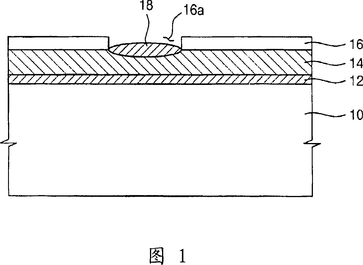
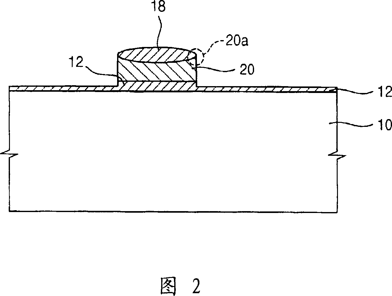
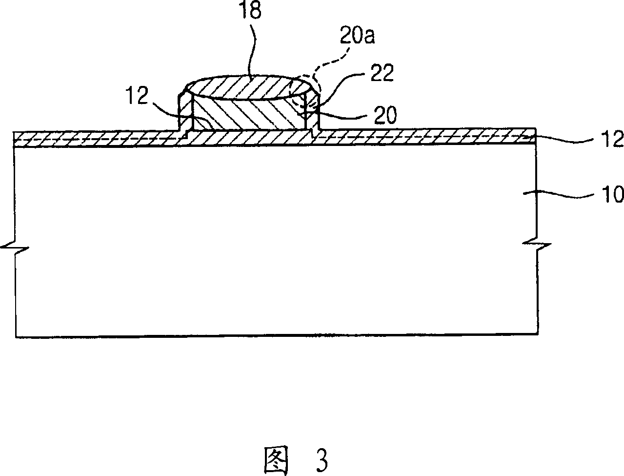
[0042] The invention will be explained in more detail hereinafter with reference to the accompanying drawings, in which exemplary embodiments of the invention are shown. This invention may, however, be embodied in many different forms and should not be construed as limited to the exemplary embodiments set forth herein. Rather, these exemplary embodiments are provided so that this disclosure will be thorough and complete. In the drawings, the size and relative sizes of layers and regions may be exaggerated for clarity.

[0043] It will be understood that when an element or layer is referred to as being "on," "connected to," and / or "coupled to" another element or layer, it can be directly on, or directly connected to, the other element or layer. to, coupled to, another element or layer, or intervening elements or layers may be present. In contrast, when an element is referred to as being "directly on," "directly connected to" and / or "directly coupled to" another element or lay...


PUM


Abstract

In a method of manufacturing a non-volatile memory device, a first gate insulation layer and a conductive layer are formed on a substrate and then the conductive layer is partially oxidized to form an oxide layer pattern. The conductive layer is partially etched using the oxide layer pattern as an etching mask to form a floating gate electrode on the first gate insulation layer and then the silicon layer is formed on the substrate including the floating gate electrode. The silicon layer is oxidized to form a tunnel insulation layer and a second gate insulation layer on a sidewall of the floating gate electrode and on a surface portion of the substrate adjacent to the floating gate electrode and then a control gate electrode is formed on the tunnel insulation layer and the second gate insulation layer. The present invention can restrain the change of an end profile of a floating gate electrode on the floating gate electrode and the change of the thickness of a gate insulation layer in the heating oxidation technics to form a tunnel oxide layer. Thus, the character of the data erasure and the data programme of the non-volatile memory device can be improved.

Description

technical field [0001] Exemplary embodiments of the present invention relate to a method of manufacturing a nonvolatile memory device, and more particularly, to a method of manufacturing a split gate type nonvolatile memory device. Background technique [0002] Semiconductor memory devices can generally be classified into volatile memory devices, such as dynamic random access memory (DRAM) or static random access memory (SRAM), and nonvolatile memory devices, such as erasable programmable read-only memory (EPROM) EPROM)), electrically erasable programmable read-only memory (EEPROM) or flash memory devices. [0003] Volatile memory devices have a relatively high operating speed for inputting and outputting data and do not retain information when powered off. Non-volatile memory devices have relatively slow operating speeds and retain information when powered off. Non-volatile memory devices are in great demand, especially for incorporation into portable devices. In a non-v...

Claims


Application Information

Patent Timeline
Patent Type & Authority Applications(China)
IPC IPC(8): H01L21/28H01L21/336H01L21/8247H01L29/788H01L29/423H01L29/51H01L27/115
CPCH01L27/11526H01L29/7881H01L21/28273H01L29/42324H01L27/105H01L27/11543H01L29/40114H10B41/40H10B41/48H01L29/66825
Inventor 郑永天权喆纯俞在玟朴在铉林智云尹仁丘
Owner SAMSUNG ELECTRONICS CO LTD
Why Eureka
Try Eureka