High current MOS device with avalanche protection and method of operation

A high-current, MOS transistor technology, applied in the semiconductor field, can solve the problems of electric-thermal failure of the device 10, hindering the pure heating limit of the device 10, etc.

Inactive Publication Date: 2007-04-11
FREESCALE SEMICON INC
View PDF0 Cites 4 Cited by
  • Summary
  • Abstract
  • Description
  • Claims
  • Application Information

AI Technical Summary

Problems solved by technology

Under high current conduction and high drain-source voltage operating conditions, parasitic bipolar transistor 38 can cause electro-thermal failure of device 10, preventing device 10 from reaching its purely thermal limit

Method used


Image

  • High current MOS device with avalanche protection and method of operation
  • High current MOS device with avalanche protection and method of operation
  • High current MOS device with avalanche protection and method of operation

Examples


Embodiment Construction

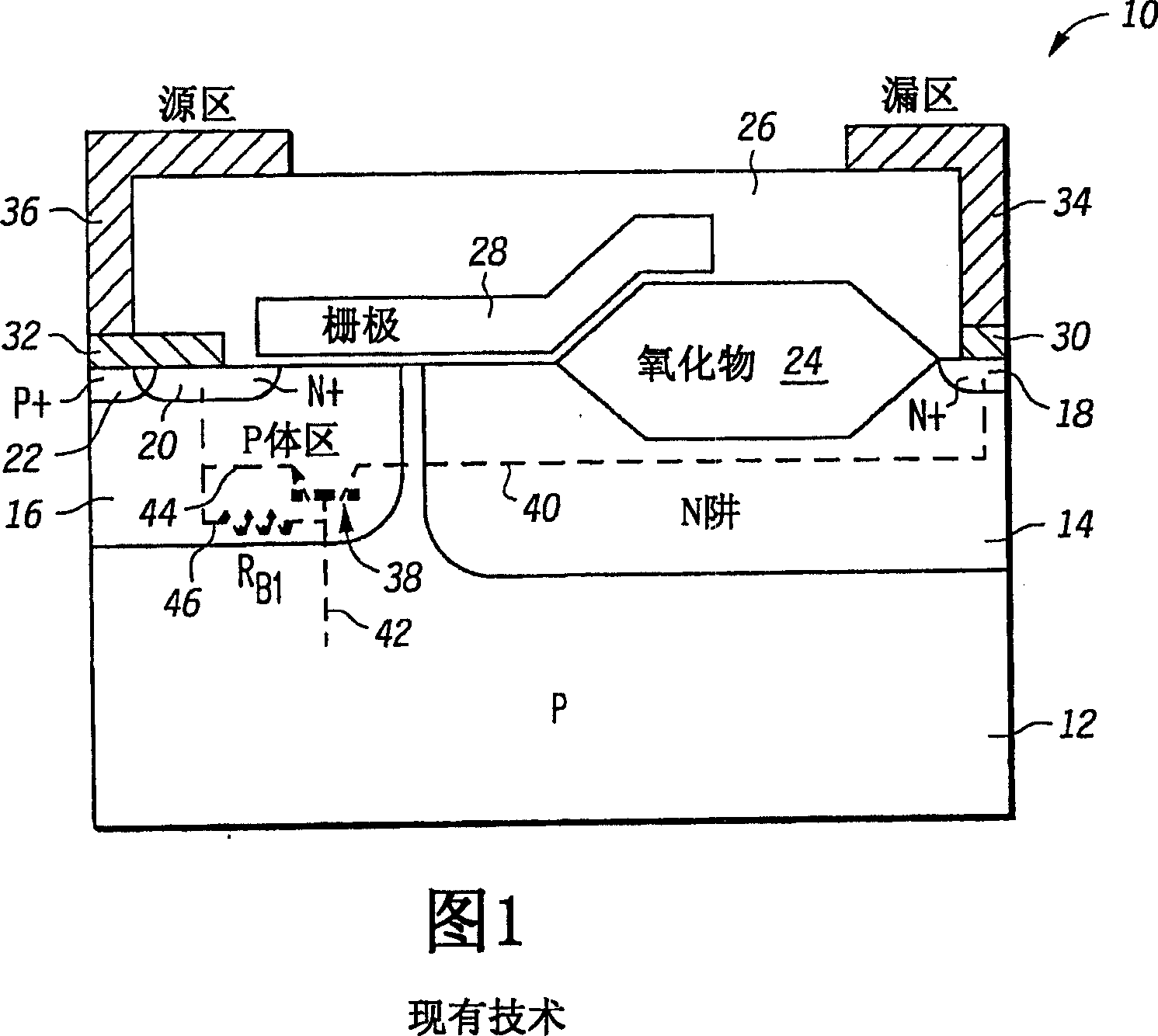
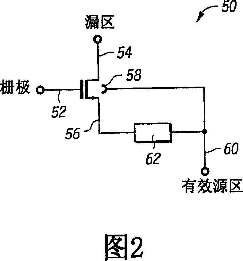
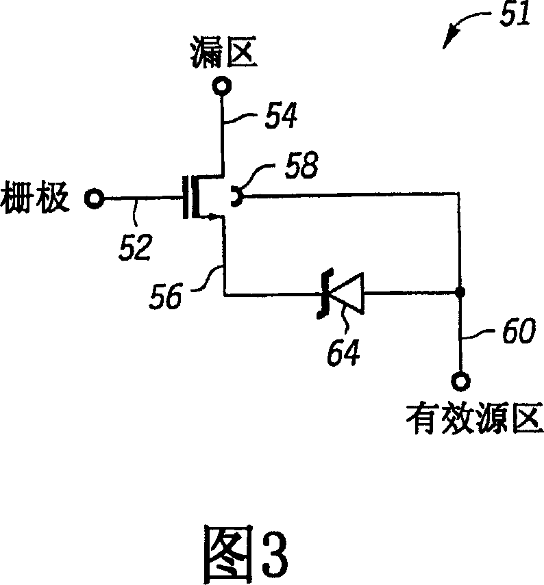
[0019] In high current applications, electron-hole pairs are generated in the drain region of the MOS transistor, causing the inherently parasitic bipolar transistor to destructively turn on. Holes pass through the body region of the MOS transistor, which has an intrinsic resistance, to the source region, which is usually held at a low voltage such as ground. The hole current causes the voltage of the body region which is the base region to rise. This rising base voltage is what causes the parasitic bipolar transistor to turn on. The channel current passes through the impedance between the source region and the body region, and the voltage between the source region and the body region as the emitter region rises, which can greatly reduce the above possibility. When the base voltage increases, it causes the emitter voltage to increase, preventing the parasitic bipolar transistor from turning on.

[0020] Therefore, in order to achieve practical thermal performance of a power ...


PUM


Abstract

Particularly in high current applications, impact ionization induced electron-hole pairs are generated in the drain (74) of an MOS transistor (51) that can cause a parasitic bipolar transistor (38) to become destructively conductive. The holes pass through the body region (76) of the MOS transistor (51), which has intrinsic resistance, to the source (80), which is typically held at a relatively low voltage, such as ground. The hole current causes a voltage to develop in the body region (76), which acts as the base (42). This increased base voltage is what can cause the parasitic bipolar transistor (38) to become conductive. The likelihood of this is greatly reduced by developing a voltage between the source (80), which acts as the emitter (44), and the body region (76) by passing the channel current through an impedance (62) between the source (80) and the body region (76). This causes the emitter voltage to increase as the base voltage is increased and thereby prevent the parasitic bipolar transistor (38) from becoming conductive.

Description

technical field [0001] The present invention relates generally to semiconductors and, more particularly, to high current MOS devices with avalanche protection and methods of operation. Background technique [0002] As power device dimensions continue to shrink, energy performance is of great concern. In fact, the size of the power MOS device is no longer limited by the working resistance, but instead is limited by the energy performance. As far as automation applications are concerned, the energy demands placed on power MOS devices can lead to significant increases in device temperature, sometimes leading to electrical failure of the corresponding devices due to snapback. Furthermore, parasitic bipolar transistors inherent in power MOS devices lead to electro-thermal failure of individual devices, preventing them from reaching the purely thermal limit of the device. [0003] FIG. 1 is a cross-sectional view of an LDMOSFET device 10 according to the prior art. LDMOSFET dev...

Claims


Application Information

Patent Timeline
Patent Type & Authority Applications(China)
IPC IPC(8): H01L29/74H01L29/76H01L27/07H01L29/08H01L29/423H01L29/78H01L31/113
CPCH01L27/0722H01L29/42368H01L29/0847H01L29/7835H01L29/76H01L31/113
Inventor 维什努·K·肯卡阿米塔瓦·博斯维贾伊·帕塔萨拉蒂祝荣华
Owner FREESCALE SEMICON INC
Why Eureka
Try Eureka