
Wiring method for printed circuitboard and printed circuitboard

A printed circuit board and wiring method technology, applied in the directions of printed circuits, printed circuit manufacturing, printed circuit components, etc., can solve the problems of low electromagnetic compatibility, large signal loop area, and increased radiation, so as to improve electromagnetic compatibility. , Reduce the signal loop area, improve the effect of electromagnetic compatibility

Inactive Publication Date: 2007-04-18
HUAWEI TECH CO LTD
View PDF0 Cites 17 Cited by
  • Summary
  • Abstract
  • Description
  • Claims
  • Application Information

AI Technical Summary

Problems solved by technology

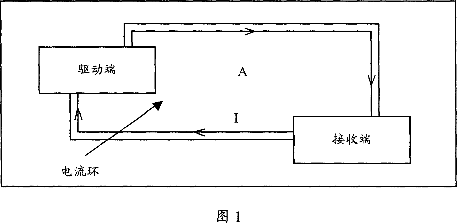
[0011] The purpose of the present invention is to provide a wiring method for printed circuit boards, which aims to solve the problems of increased radiation and low electromagnetic compatibility due to the large signal loop area when wiring printed circuit boards

Method used


Image

  • Wiring method for printed circuitboard and printed circuitboard
  • Wiring method for printed circuitboard and printed circuitboard
  • Wiring method for printed circuitboard and printed circuitboard

Examples


Embodiment Construction

[0037] In order to make the object, technical solution and advantages of the present invention clearer, the present invention will be further described in detail below in conjunction with the accompanying drawings and embodiments. It should be understood that the specific embodiments described here are only used to explain the present invention, not to limit the present invention.

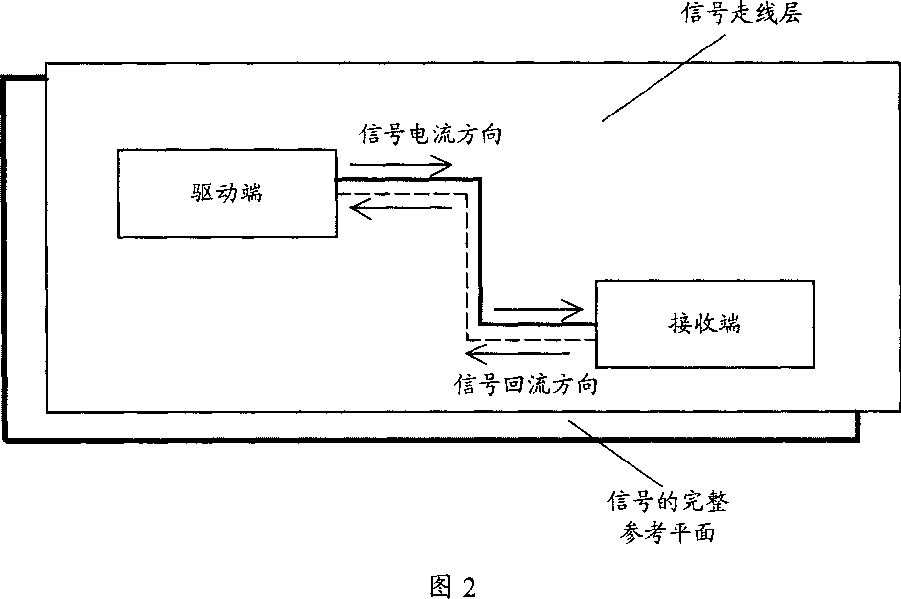
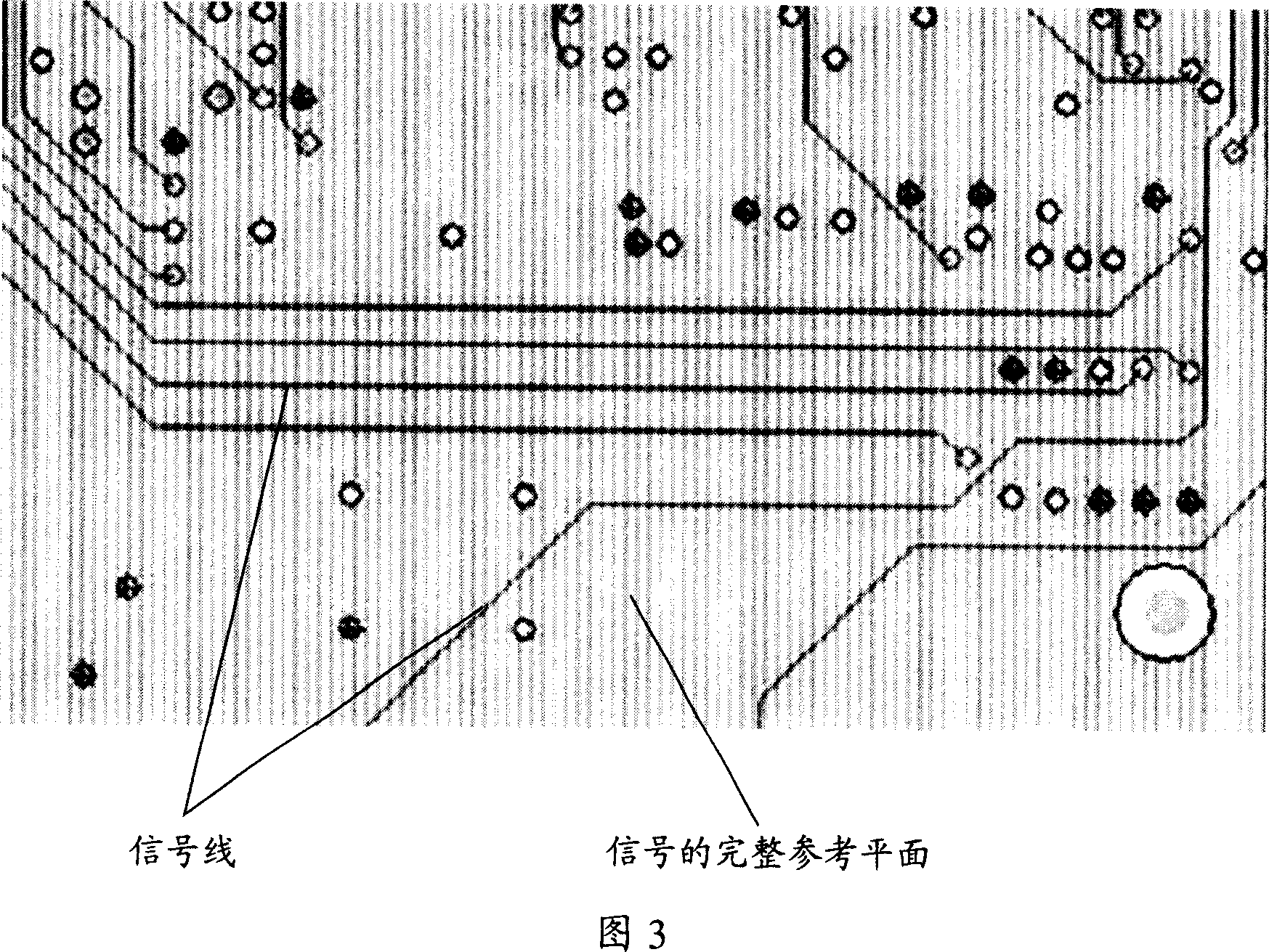
[0038] When wiring the printed circuit board in the present invention, the power supply wiring and the ground wire are arranged side by side, and the way of walking along with the signal line is provided to provide a return path for the signal, which effectively reduces the loop area of ​​the signal and improves the printed circuit. board capacitive compatibility.

[0039] The signal return method can be divided into two types: power return and ground return. Take a low-voltage transistor-transistor-logic (LVTTL) level signal with a supply voltage of 3.3V as an example, and its input and output are...


PUM


Abstract

The invention is applied to PCB making field, providing a PCB routing method and the PCB. As routing, it routes power and ground lines in parallel with signal lines. And it provides nearby power and ground return paths for signals, reducing signal circuit area and improving PCB EMC. Besides, it improves PCB EMC effect by placing filter capacitors in the signal layer transfer position on this basis according to actual requirements, or gridding power and ground network, or placing filter capacitors between power and ground network traces.

Description

technical field [0001] The invention belongs to the field of printed circuit board manufacture, and in particular relates to a wiring method for a printed circuit board and the printed circuit board. Background technique [0002] With the development of science and technology, the signal rate of electronic products is getting faster and faster, the noise tolerance is getting lower and lower, signal integrity (Signal Integrity, SI), power integrity (Power Integrity, PI), electromagnetic compatibility (Electromagnetic Compatibility) Magnetic Compatibility, EMC) problems are becoming more and more prominent. People usually require electronic products to have electromagnetic compatibility, which refers to the ability of electronic equipment or systems to operate in their electromagnetic environment without causing unbearable electromagnetic interference to any equipment in their environment. Therefore, EMC includes two requirements: on the one hand, it means that the electromag...

Claims


Application Information

Patent Timeline
IPC IPC(8): H05K3/00H05K1/11
Inventor 郑姚兴
Owner HUAWEI TECH CO LTD
Learn More