A stacking type wafer packaging structure

A chip packaging and stacking technology, applied in the direction of semiconductor/solid-state device components, semiconductor devices, electrical components, etc., can solve the problems of inability to be precise and the height cannot be reduced, and achieve the effect of reducing the height and volume.

Inactive Publication Date: 2007-05-16
CHIPMOS TECH INC
View PDF0 Cites 11 Cited by
  • Summary
  • Abstract
  • Description
  • Claims
  • Application Information

AI Technical Summary

Problems solved by technology

However, since the spacer 140 is disposed in the stacked chip package structure 100, its height cannot be reduced, and the requirement of compactness cannot be met.

Method used


Image

  • A stacking type wafer packaging structure
  • A stacking type wafer packaging structure
  • A stacking type wafer packaging structure

Examples


Embodiment Construction

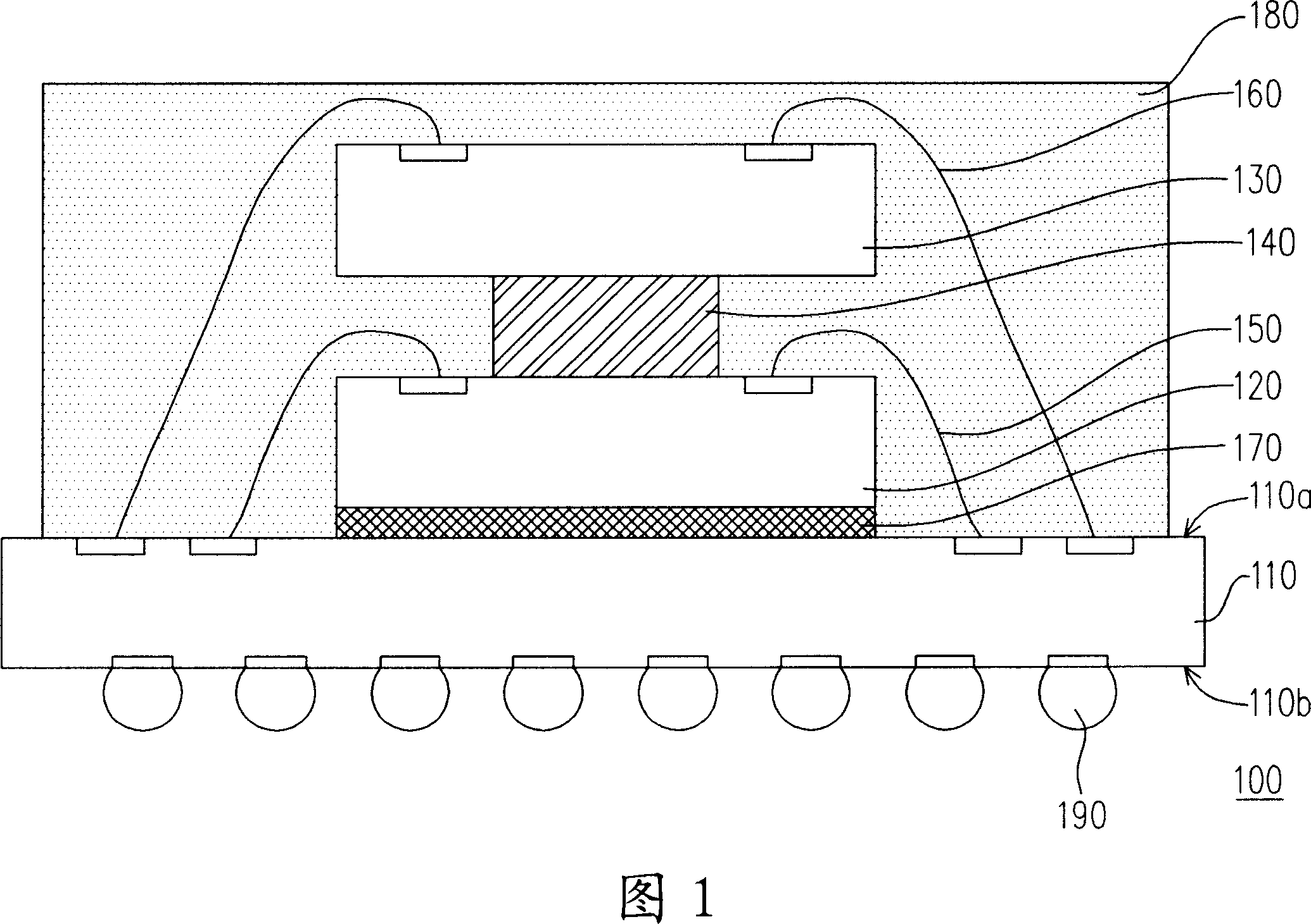
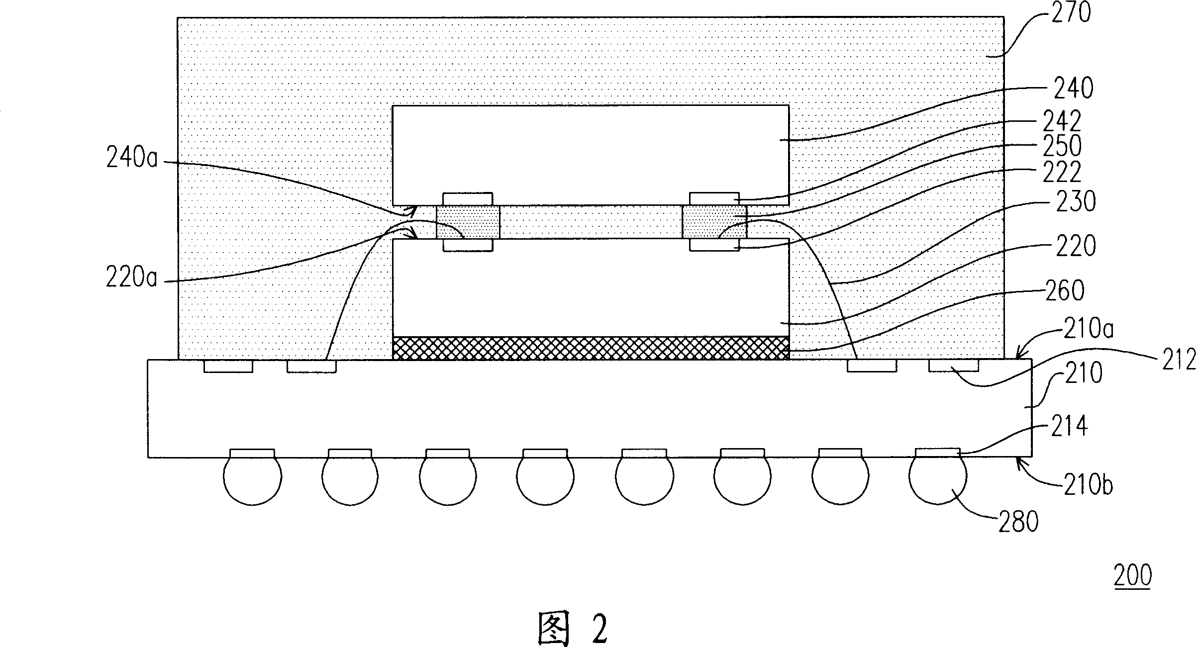
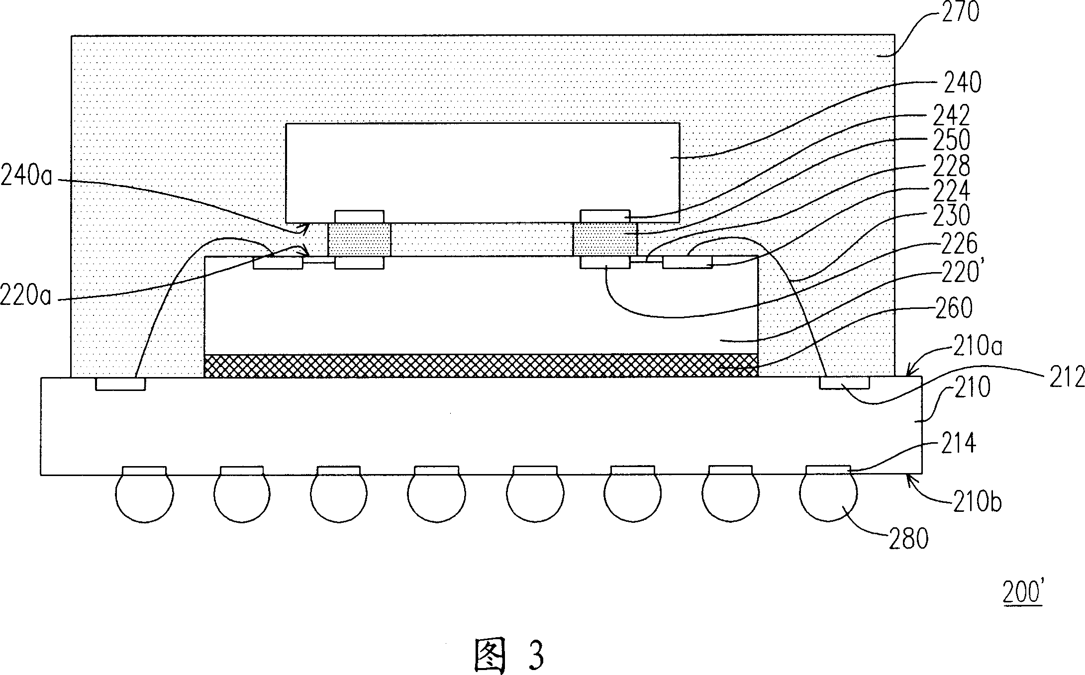
[0042] FIG. 2 is a schematic cross-sectional view of the first embodiment of the stacked chip package structure of the present invention. Referring to FIG. 2 , the stacked chip package structure 200 of the present invention mainly includes a substrate 210 , a first chip 220 , a plurality of bonding wires 230 , a second chip 240 and a plurality of B-stage conductive bumps 250 . A plurality of first solder pads 212 and a plurality of second solder pads 214 are respectively disposed on the first surface 210 a and the second surface 210 b of the substrate 210 . The first chip 220 is disposed on the first surface 210 a of the substrate 210 , and a plurality of third bonding pads 222 are disposed on the active surface 220 a. In an embodiment of the present invention, the first chip 220 is adhered on the substrate 210 through an adhesive layer 260 . However, the first chip can also be fixed on the substrate 210 by other methods, and the present invention does not impose any limitati...


PUM


Abstract

The static wafer package structure comprises: a substrate with a first wafer, multiple wires, a second wafer above the first one with multiple second pads on its active surface, and multiple B-stage conductive bumps. Wherein, these first welding pads are arranged on the active surface of the first wafer to connect with both substrate and the second pad; and bumps cover part wires.

Description

technical field [0001] The present invention relates to a chip package structure, and in particular to a stacked chip package structure. Background technique [0002] In today's highly informationized society, the market for multimedia applications continues to expand rapidly. Integrated circuit packaging technology also needs to cooperate with the digitalization, networking, regional connection and user-friendly development of electronic devices. In order to meet the above requirements, it is necessary to strengthen the requirements of high-speed processing, multi-functionality, accumulation, miniaturization, weight reduction and low price of electronic components. Therefore, different types of high-density packages have been developed, such as Ball grid arrays (BGA), Chip Scale Package (CSP), Flip Chip and stacked multi-chip packages. Packaging modules. [0003] FIG. 1 is a schematic cross-sectional view of a conventional stacked chip package structure. Referring to FI...

Claims


Application Information

Patent Timeline
Patent Type & Authority Applications(China)
IPC IPC(8): H01L25/00H01L23/488
CPCH01L2924/15311H01L2224/16145H01L2224/32145H01L2224/32225H01L2224/48091H01L2224/48227H01L2224/73265H01L2224/73207H01L2924/00014H01L2924/00
Inventor 沈更新
Owner CHIPMOS TECH INC
Why Eureka
Try Eureka