Method of barrier layer surface treatment to enable direct copper plating on barrier metal

A metal surface and metal technology, applied in the field of barrier layer surface treatment, can solve the problem of difficult seed crystal stage coverage and other problems

Inactive Publication Date: 2007-05-16
APPLIED MATERIALS INC
View PDF3 Cites 8 Cited by
  • Summary
  • Abstract
  • Description
  • Claims
  • Application Information

AI Technical Summary

Problems solved by technology

However, as feature sizes get smaller, it is difficult to have proper seed phase coverage with PVD techniques ...

Method used


Image

  • Method of barrier layer surface treatment to enable direct copper plating on barrier metal
  • Method of barrier layer surface treatment to enable direct copper plating on barrier metal
  • Method of barrier layer surface treatment to enable direct copper plating on barrier metal

Examples


Embodiment Construction

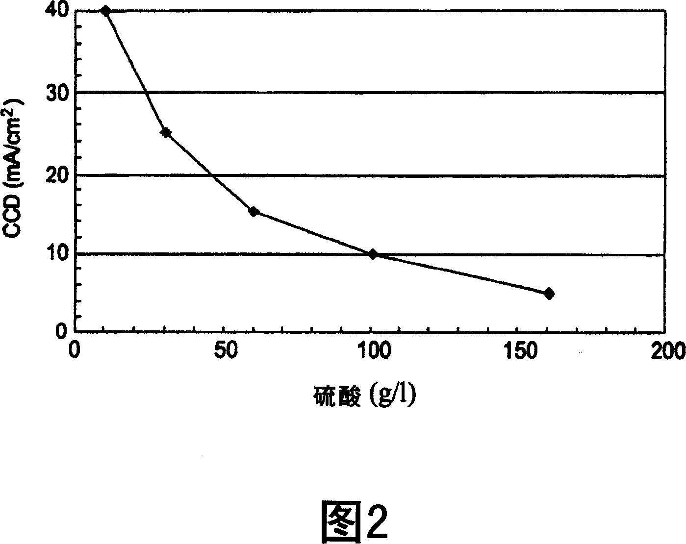
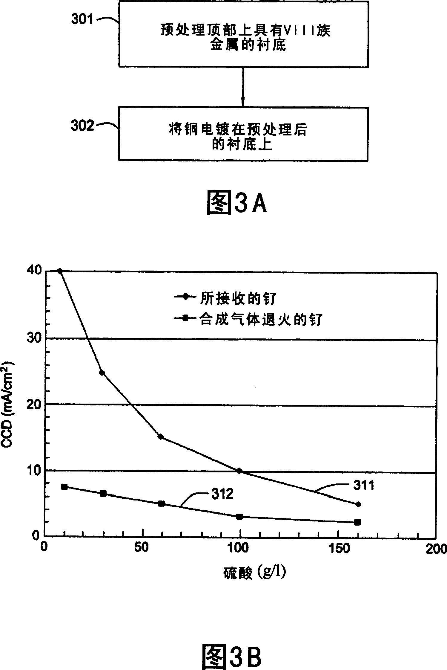
[0020] Ruthenium (Ru) thin films deposited by CVD, ALD or PVD may be potential candidates for seedless diffusion barriers between intermetal dielectrics (IMDs) and copper interconnects for sub-45nm technologies. Ruthenium is a Group VIII metal with low resistivity (resistivity ~7 μW-cm) and high thermal stability (high melting point ~2300°C). Ruthenium is relatively stable even in the presence of oxygen and water at ambient temperature. Ruthenium has twice the thermal and electrical conductivity of tantalum (Ta). Ruthenium does not form alloys with copper below 900°C and exhibits good adhesion to copper. Accordingly, the semiconductor industry has become interested in using ruthenium as a copper barrier layer. The low resistivity of ruthenium is an advantage when attempting to fill ruthenium-coated features with copper without a seed layer.

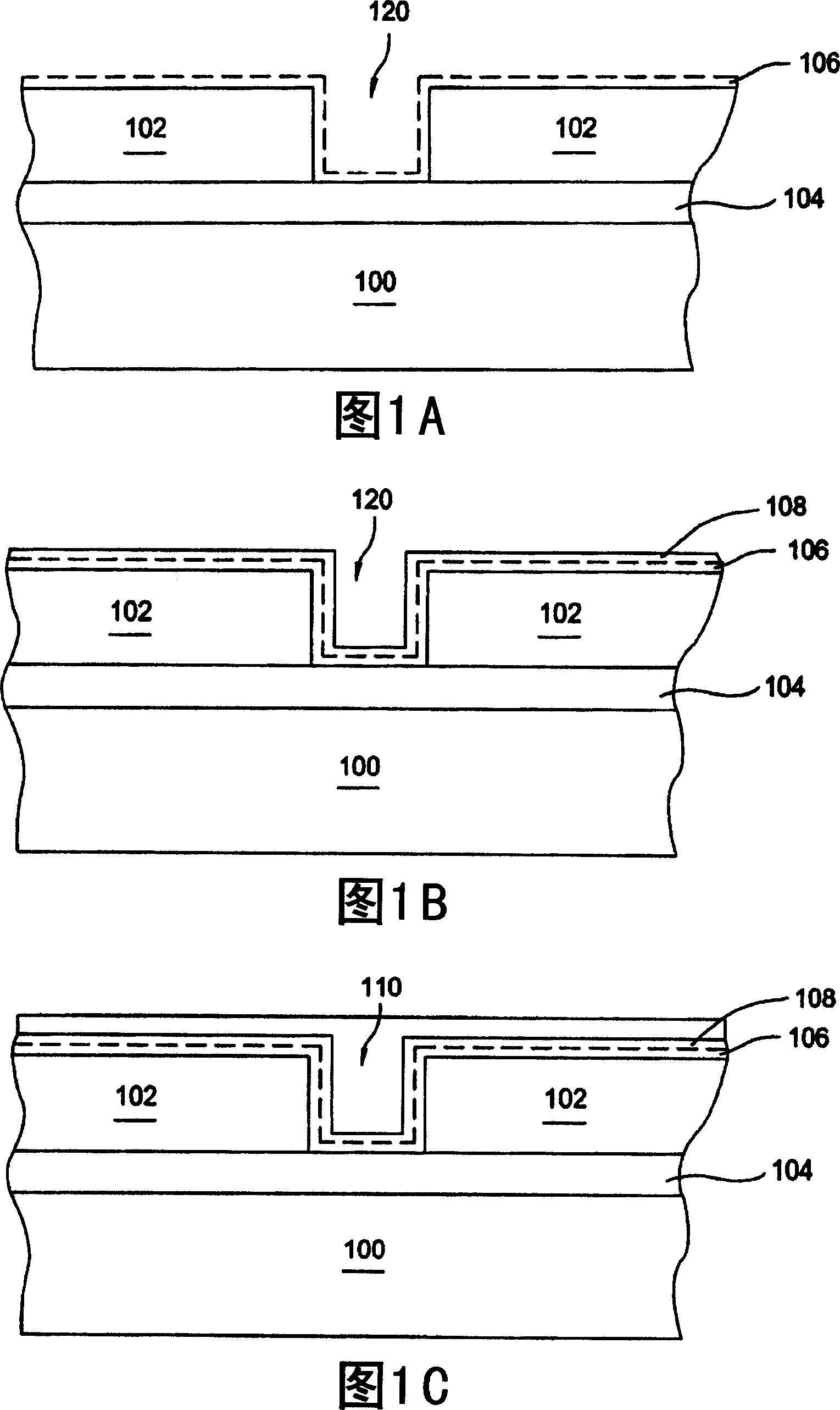
[0021] 1A-1C illustrate cross-sectional views of a substrate at various stages in a copper interconnect fabrication sequence incorpor...


PUM


Abstract

The invention discloses embodiments of a method of barrier layer surface treatment to enable direct copper plating without copper seed layer. In one embodiment, a method of plating copper on a substrate with a group VIII metal layer on top comprises pre-treating the substrate surface by removing a group VIII metal surface oxide layer and/or surface contaminants and plating copper on the pre-treated group VIII metal surface. Pre-treating the substrate can be accomplished by annealing the substrate in an environment with a hydrogen-containing gas environment and/or a non-reactive gas(es) to group VIII, by a cathodic treatment in an acid-containing bath, or by immersing the substrate in an acid-containing bath.

Description

technical field [0001] Embodiments of the invention generally relate to methods of barrier surface treatment that enable direct copper plating on barrier metals. Background technique [0002] Sub-quarter-micron, multilayer metallization is one of the key technologies for next-generation very large-scale integration (VLSI) and very large-scale integration (ULSI) semiconductor devices. The multilayer interconnects at the heart of this technology require filling contacts, vias, lines, and other features formed in voids with high aspect ratios. Reliable formation of these features is very important to the success of both VLSI and ULSI, as well as to the ongoing effort to increase circuit density and quality on individual substrates and dies. [0003] As circuit density increases, the widths of contacts, vias, lines, other features, and intervening dielectric material decrease to less than 65 nm, while the thickness of the dielectric layer remains substantially constant, resulti...

Claims


Application Information

Patent Timeline
IPC IPC(8): C25D5/34
Inventor 孙志文何人人
Owner APPLIED MATERIALS INC
Why Eureka
Try Eureka