
Method and device to access multicenter IDE bus by data bus

A data bus, multi-channel technology, applied in electrical digital data processing, instruments, etc., can solve the problems of insufficient scalability, inability to miniaturize circuit boards, and inability to use, to avoid mutual interference, improve convenience and scope of application. Effect

Active Publication Date: 2007-05-23
PHISON ELECTRONICS
View PDF0 Cites 0 Cited by
  • Summary
  • Abstract
  • Description
  • Claims
  • Application Information

AI Technical Summary

Problems solved by technology

[0003] Furthermore, many data storage devices currently on the market use Integrated Drive Electronics (IDE for short), and the integrated drive electronics interface is an 8-bit or 16-bit interface for controlling data storage devices, and its control chip is made on the periphery On the device, the adapter card itself is simpler and lower in price, so many data storage devices use the integrated drive electronic interface, but it is often limited by the hardware design of the processor that does not support it, or the expansion is not enough to make the integrated drive electronic interface Interface support is limited
However, today's electronic products tend to be light, thin, short, and small. Therefore, when multiple bus interfaces are installed on the circuit board, it will occupy too much space on the circuit board, making the circuit board unable to be miniaturized, and thus preventing the electronic products from trending Light, thin, short, and small development, and when multiple bus interfaces are soldered, it is easy to cause poor soldering and cannot be used, which reduces the pass rate of electronic products and increases the cost

Method used


Image

  • Method and device to access multicenter IDE bus by data bus
  • Method and device to access multicenter IDE bus by data bus
  • Method and device to access multicenter IDE bus by data bus

Examples


Embodiment Construction

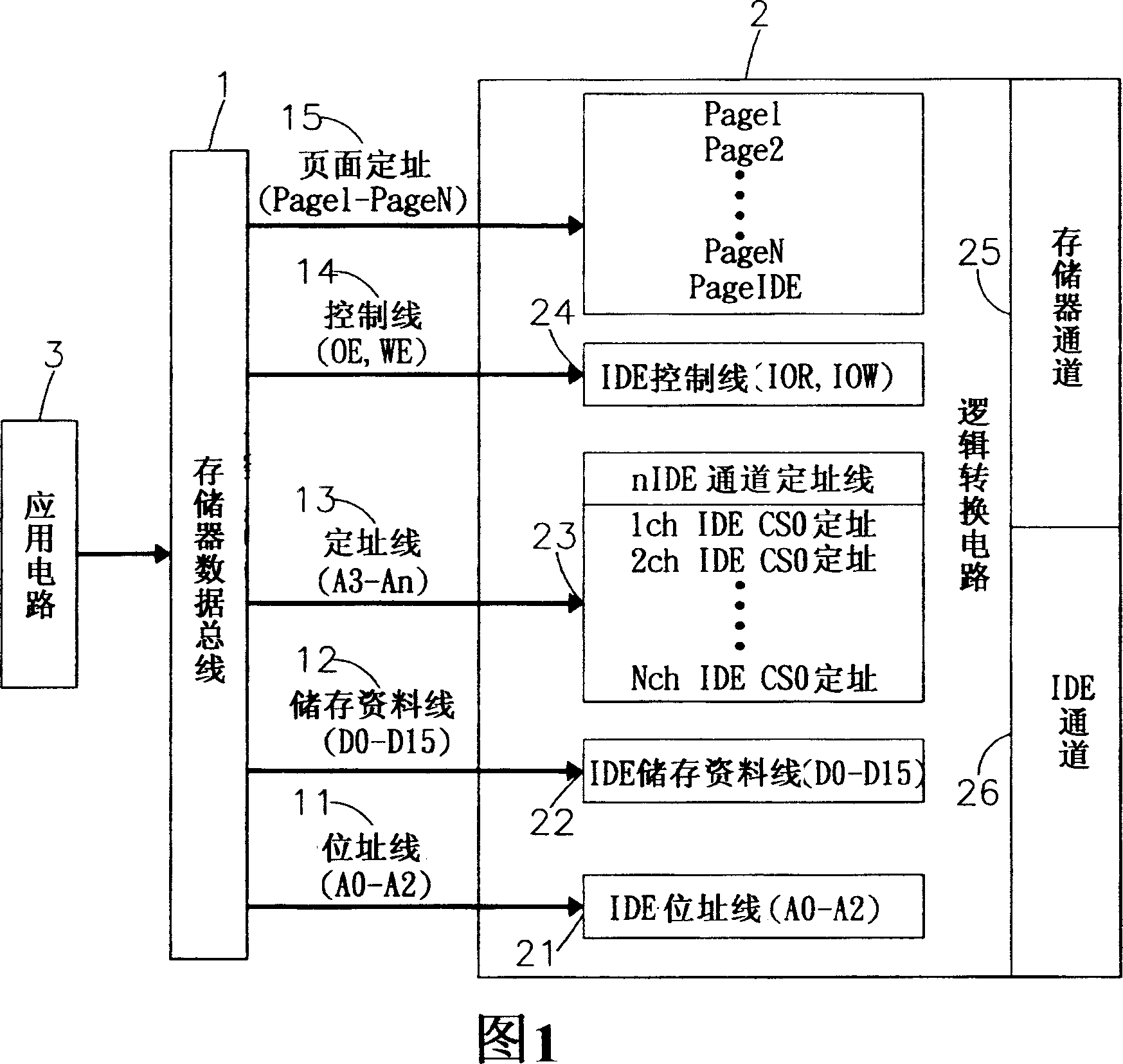
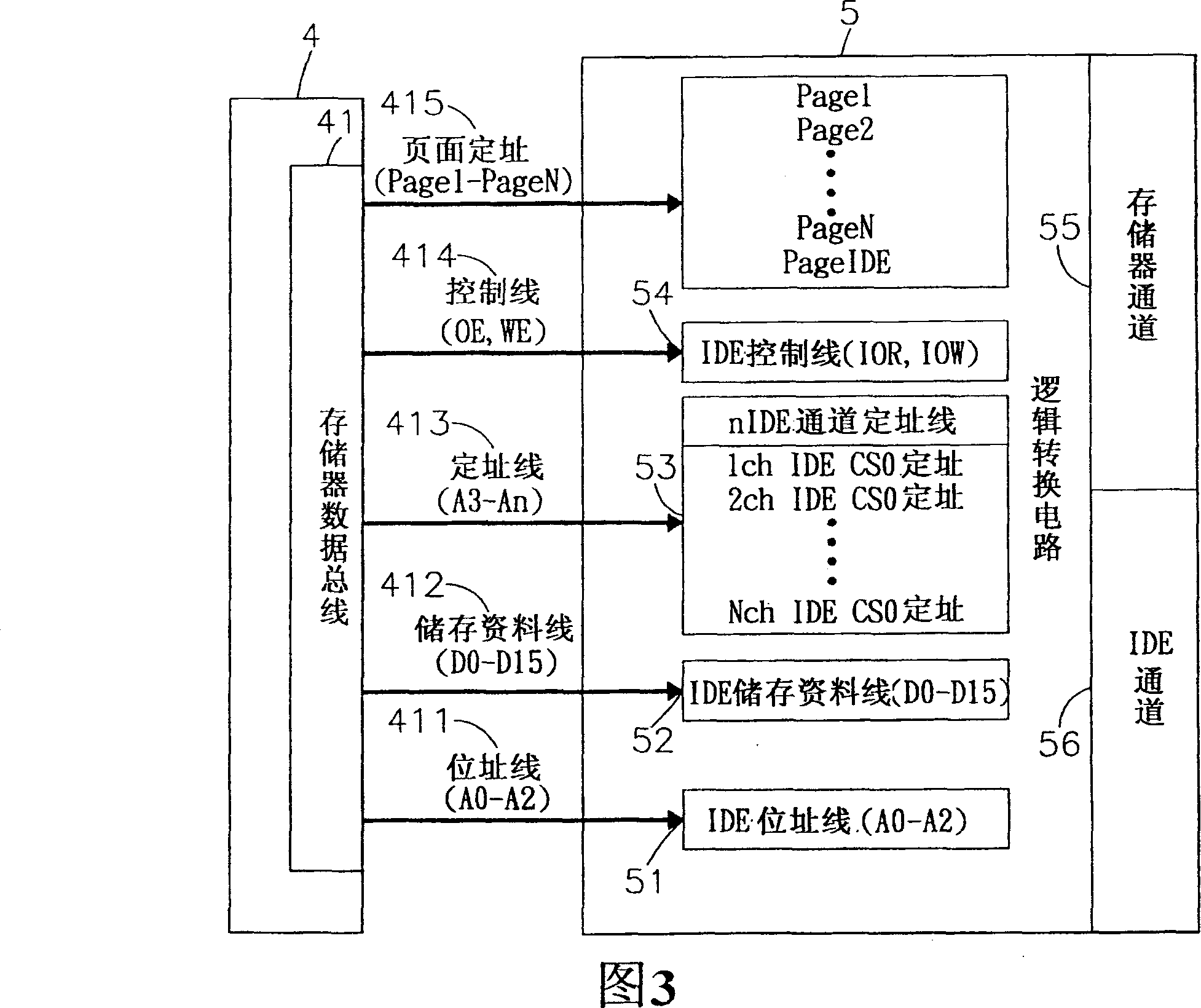
[0039] Please refer to Fig. 1, which is a block diagram of a preferred embodiment of the present invention. It can be clearly seen from the figure that the device for utilizing a memory data bus to access a multi-channel IDE bus of the present invention includes a memory data bus 1 and a memory data bus 1. Logic conversion circuit 2, wherein:

[0040] The memory data bus 1 is electrically connected to the application circuit 3, and the memory data bus 1 is provided with address lines 11 (A0-A2), storage data lines 12 (D0-D15), address lines 13 (A3-An), Control lines 14 (OE, WE) and page addressing 15 (Pagel-PageN).

[0041] The logic conversion circuit 2 is electrically connected to the memory data bus 1, and the logic conversion circuit 2 is provided with IDE address lines 21 (A0-A2), IDE storage data lines 22 (D0-D15), and n IDE channel address lines 23 (1ch IDE_CS0-nch IDE_CS0) and IDE control lines 24 (IDE_IOW, IDE_IOR), and the logic conversion circuit 2 is connected wit...


PUM


Abstract

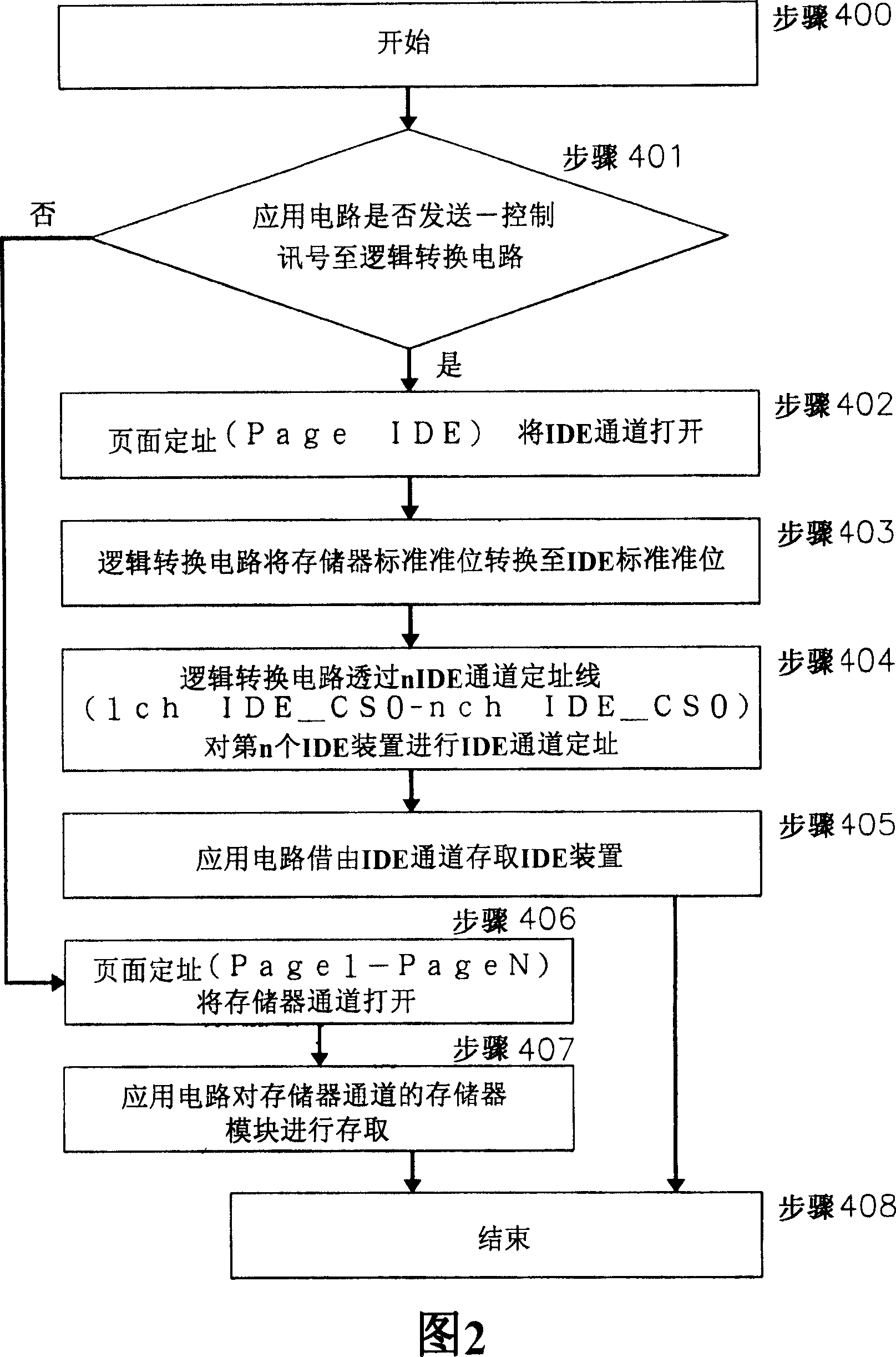
The invention is a method and device of accessing to multi-channel IDE bus by a memory data bus, including memory data bus and logic conversion circuit. The memory data bus has the bit-address line, data-storage line, decide-address line, control line and page decide-address, and logical conversion circuit and memory data bus are electric connectivity, and it has the IDE address line, IDE data-storage line, n- IDE channel decide-address line and IDE control line, and links IDE channel and memory channel. While the page decide-address opens the IDE channel, the logic conversion circuit can convert non-IDE standard bit to IDE standard bit, and processes channel decide-address through n- IDE channel decide-address lines, so it can access IDE devices of multiple IDE channels via memory data bus.

Description

technical field [0001] The present invention is a method and device for accessing a multi-channel IDE bus by using a memory data bus, which uses a logic conversion circuit to convert non-IDE standard levels to IDE standard levels, allowing the memory data bus to access multiple IDE channels IDE installation. Background technique [0002] With the advancement of the electronic industry and the rapid development of electronic technology applications, the leading markets of the semiconductor industry and the information electronics industry continue to grow vigorously, resulting in significant changes in quite a few application levels, and more and more electronic products are being used frequently. The application in daily life brings not only scientific and technological achievements, but also improves the quality of human life and changes the mode of life. In the application of many different electronic products, many different types of memories must be used. In order to pr...

Claims


Application Information

Patent Timeline
Patent Type & Authority Applications(China)
IPC IPC(8): G06F13/40
Inventor 沈峰民陈荣伟
Owner PHISON ELECTRONICS
Learn More