Supercharge Your Innovation With Domain-Expert AI Agents!

Radiating structure of coverting element of plasma display

A technology of plasma display and conversion element, applied in cooling/ventilation/heating transformation, solid cathode components, etc., can solve the problems of inability to absorb heat evenly, long time required for heat dissipation, poor heat dissipation effect, etc., to avoid disadvantages Influence, prevent components from being exposed, the effect of good effect

Inactive Publication Date: 2007-06-13
LG ELECTRONICS(NANJING) PLASMA CO LTD
View PDF0 Cites 0 Cited by
  • Summary
  • Abstract
  • Description
  • Claims
  • Application Information

AI Technical Summary

Problems solved by technology

[0020] However, the heat dissipation structure of the existing conversion elements 1 and 2 has a problem as can be seen from the accompanying drawings, that is, the two FET conversion elements as heat sources are very close to each other and are installed side by side on one side of the synchronous radiator 70 on, resulting in poor heat dissipation
[0021] That is, since the heat conversion elements are concentratedly installed on one face of the synchronous radiator 70, heat cannot be absorbed evenly, and at the same time, the heat released between the elements can also cause adverse effects.
[0022] It should also be pointed out that since only one of the four faces of the FET conversion elements 1 and 2 is in contact with the synchronous heat sink 70, the time required for heat dissipation is relatively long.

Method used


Image

  • Radiating structure of coverting element of plasma display
  • Radiating structure of coverting element of plasma display
  • Radiating structure of coverting element of plasma display

Examples


Embodiment Construction

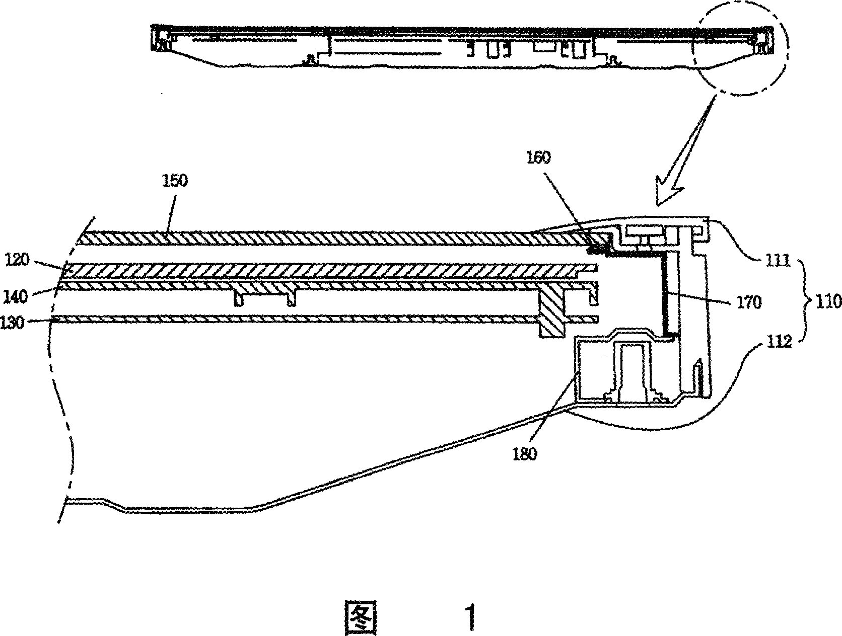
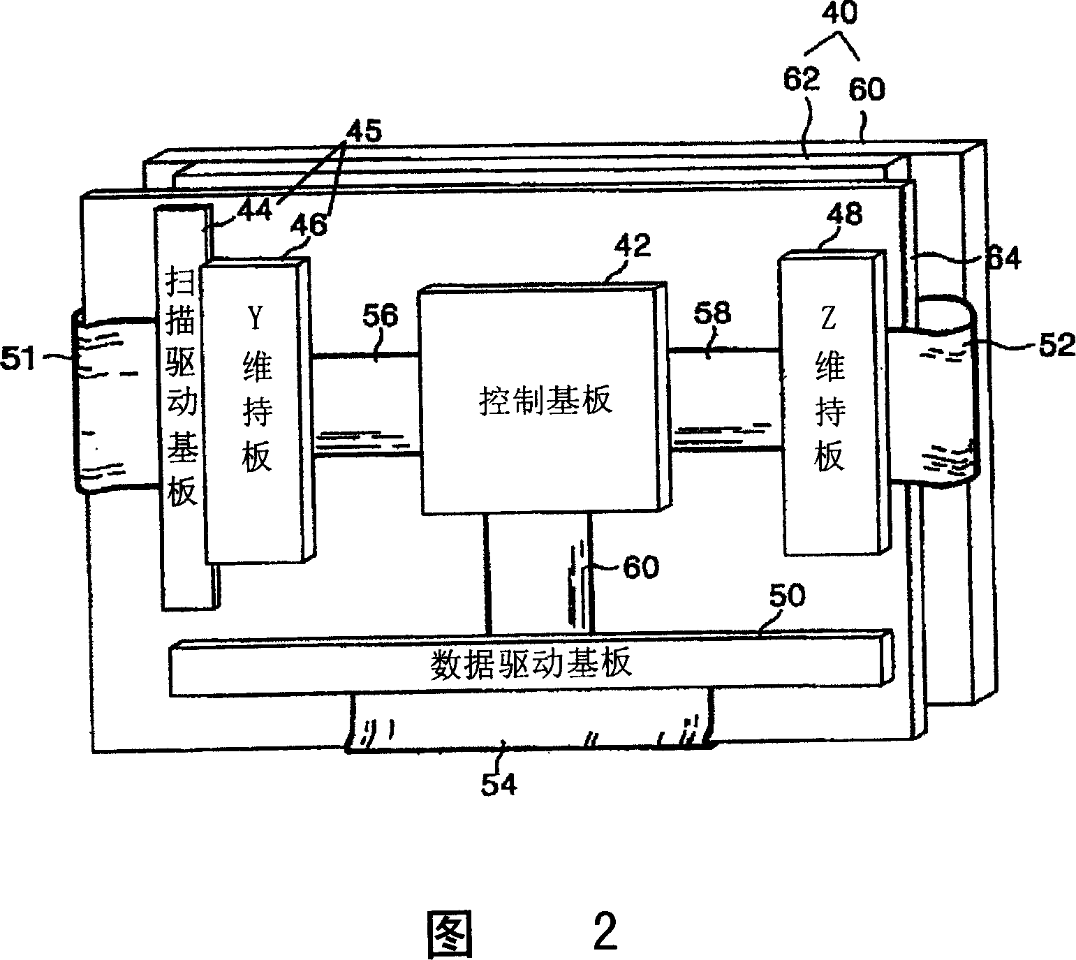
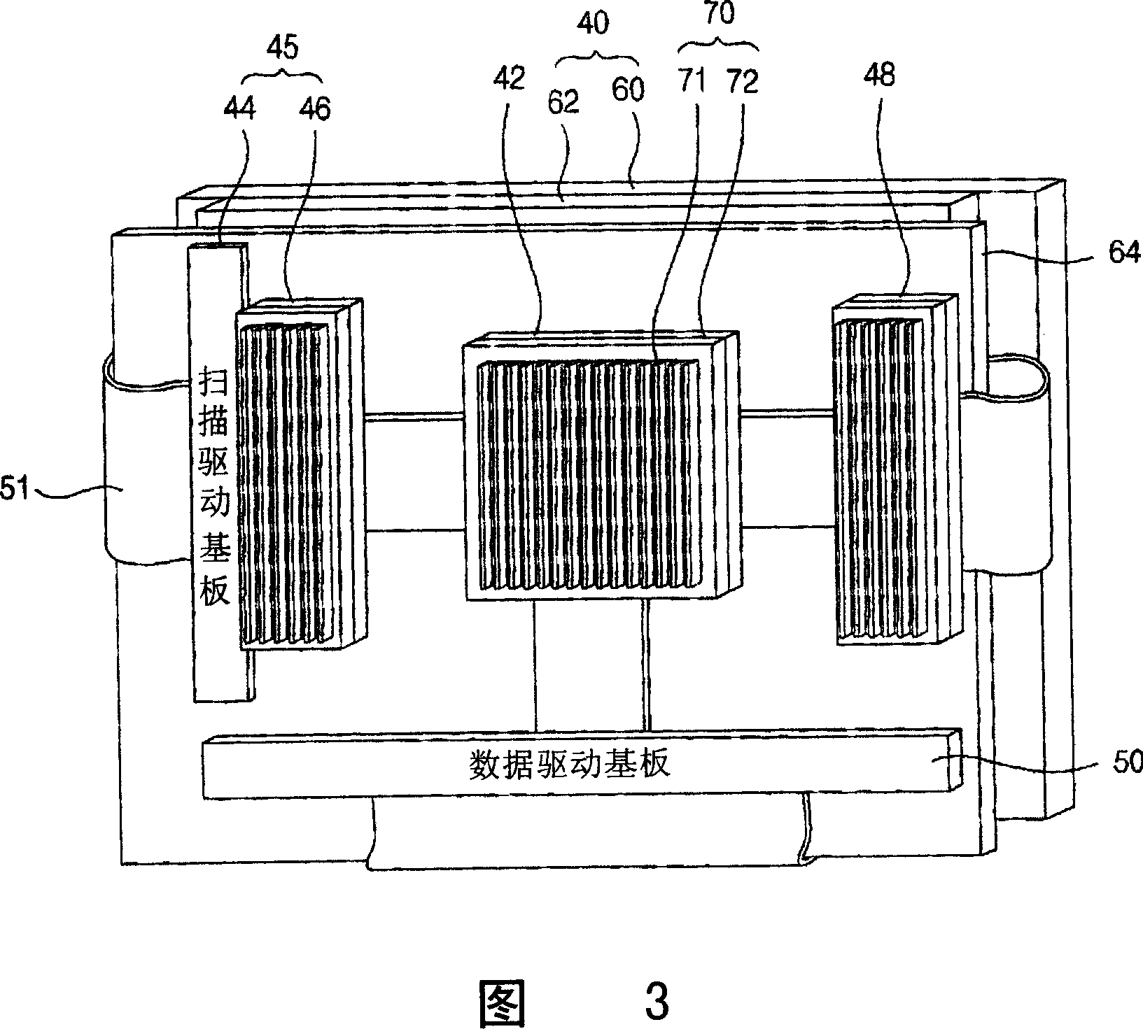
[0045] Hereinafter, specific embodiments of the heat dissipation structure of the conversion element of the plasma display according to the present invention will be described in detail with reference to FIGS. 5 to 8 .

[0046]As shown in FIG. 5 , it is a schematic plan view of the synchronous heat sink installation state of the FET element in the embodiment of the present invention. FIG. 6 is a schematic diagram of a separated state of the cooling fins forming the mounting grooves in the embodiment of the present invention. As shown in Fig. 7a and 7b, the heat conduction situation of the existing heat dissipation structure is compared with the heat conduction situation of the heat dissipation structure of the present invention. FIG. 8 is a schematic diagram of the installation state of the FET element in another embodiment of the present invention.

[0047] First, let's look at the mounting structure of the synchronous heat sink for dissipating heat from the conversion eleme...


PUM


Abstract

The invention is for the heat dispersing structure of the transforming components of plasma display, the invention includes the driving device that is formed by several substrates, the function of which is to drive the wirings of each electrode of plasma display; several FET transforming components that are installed on each substrates, the function of which is to provide various pulse to the above-said electrode wirings; a synchro radiator with heat dispersing rod is designed at one side of the substrates in order to bring and release the heat quantity it produces by above-said transforming component outwards, then forms a plasma display that can disperse heat quantity through the installation of transforming components. The features of the invention are the above-said several transforming components that are installed respectively on the different sides of the synchro radiator. The purpose of the invention is to change the installation position of all high voltage transforming components of plasma display in the synchro radiator, when the circuit of the plasma display drives, the heat quantity it produces by high voltage transforming component can be released quickly and efficiently, and then avoid the disadvantageous effect caused by the heat quantity to the driving circuit.

Description

technical field [0001] The present invention relates to the technology of heat dissipation structure of circuit elements of plasma display (PDP). In particular, when the PDP screen is driven, the present invention can timely and effectively release the heat generated by the FET conversion element of the circuit part during operation, and a heat dissipation structure of the conversion element of the plasma display. Background technique [0002] Usually, the working principle of a plasma display is that the partition wall formed between the front substrate and the rear substrate constitutes a unit cell, and neon gas (Ne), helium gas (He) or a mixed gas with neon and helium is injected into the cell. (Ne+He)-based discharge gas and inert gas containing a small amount of xenon. When the high-frequency voltage is discharged, the inert gas emits vacuum ultraviolet rays (Vacuum Ultraviolet rays) to make the phosphors formed between the partition walls emit light to display images....

Claims


Application Information

Patent Timeline
Patent Type & Authority Applications(China)
IPC IPC(8): H01J17/28H05K7/20
Inventor 朴相敏
Owner LG ELECTRONICS(NANJING) PLASMA CO LTD
Features
  • R&D
  • Intellectual Property
  • Life Sciences
  • Materials
  • Tech Scout
  • Unparalleled Data Quality
  • Higher Quality Content
  • 60% Fewer Hallucinations
Learn More