Semiconductor device, manufacturing method for semiconductor device, electronic component, circuit board, and electronic device

A technology for electronic components and manufacturing methods, which is applied in the fields of semiconductor/solid-state device manufacturing, semiconductor/solid-state device components, semiconductor devices, etc. Effect

Inactive Publication Date: 2007-06-13
SEIKO EPSON CORP
View PDF2 Cites 3 Cited by
  • Summary
  • Abstract
  • Description
  • Claims
  • Application Information

AI Technical Summary

Problems solved by technology

[0015] After the gold layer is formed by electroplating, it is necessary to perform etching and cleaning processes separately, resulting in a decrease in manufacturing efficiency

Method used


Image

  • Semiconductor device, manufacturing method for semiconductor device, electronic component, circuit board, and electronic device
  • Semiconductor device, manufacturing method for semiconductor device, electronic component, circuit board, and electronic device
  • Semiconductor device, manufacturing method for semiconductor device, electronic component, circuit board, and electronic device

Examples


Embodiment Construction

[0060] Embodiments of a semiconductor device, a method of manufacturing a semiconductor device, an electronic component, a circuit board, and an electronic device according to the present invention will be described below with reference to FIGS. 1 to 7 .

[0061] [semiconductor device]

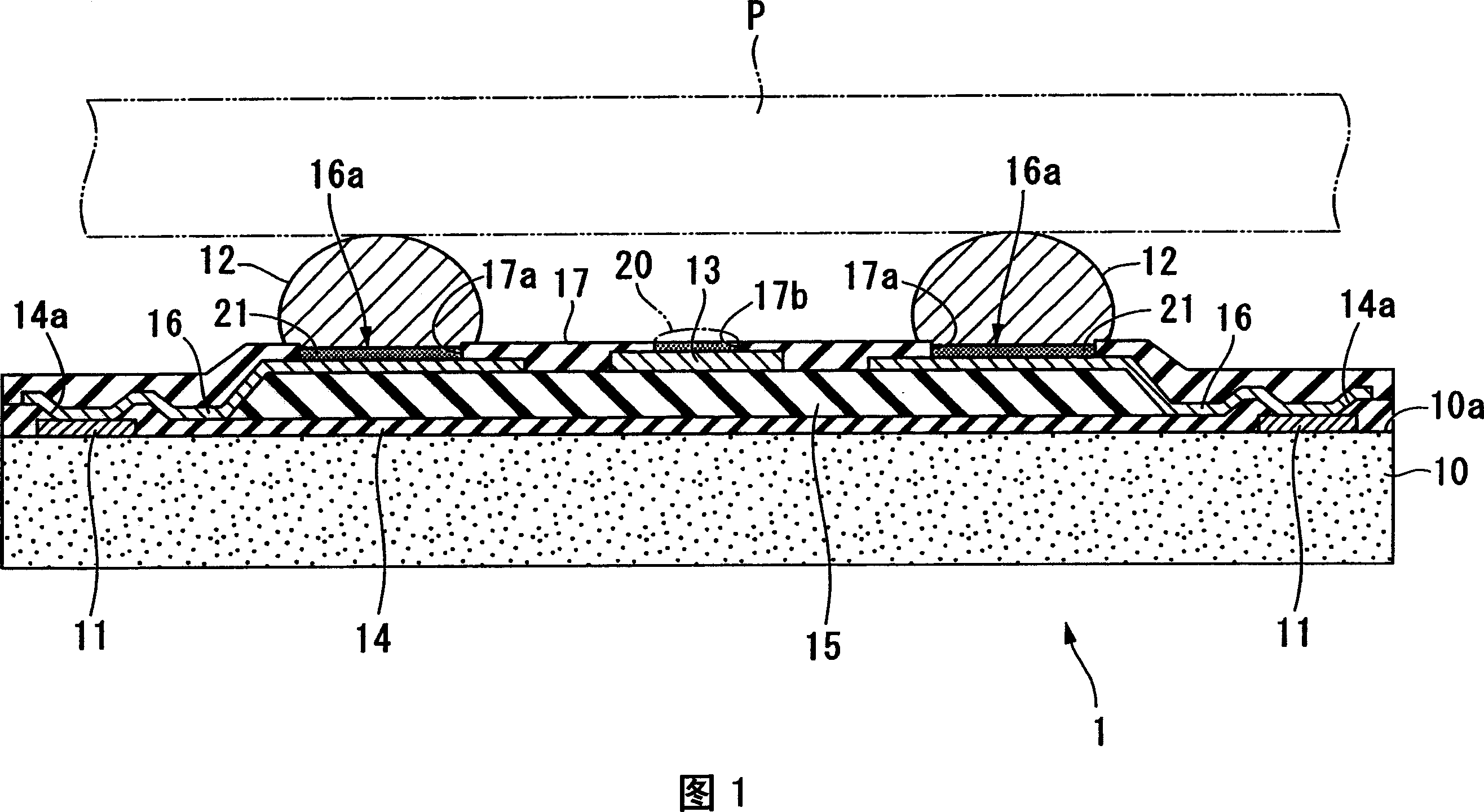
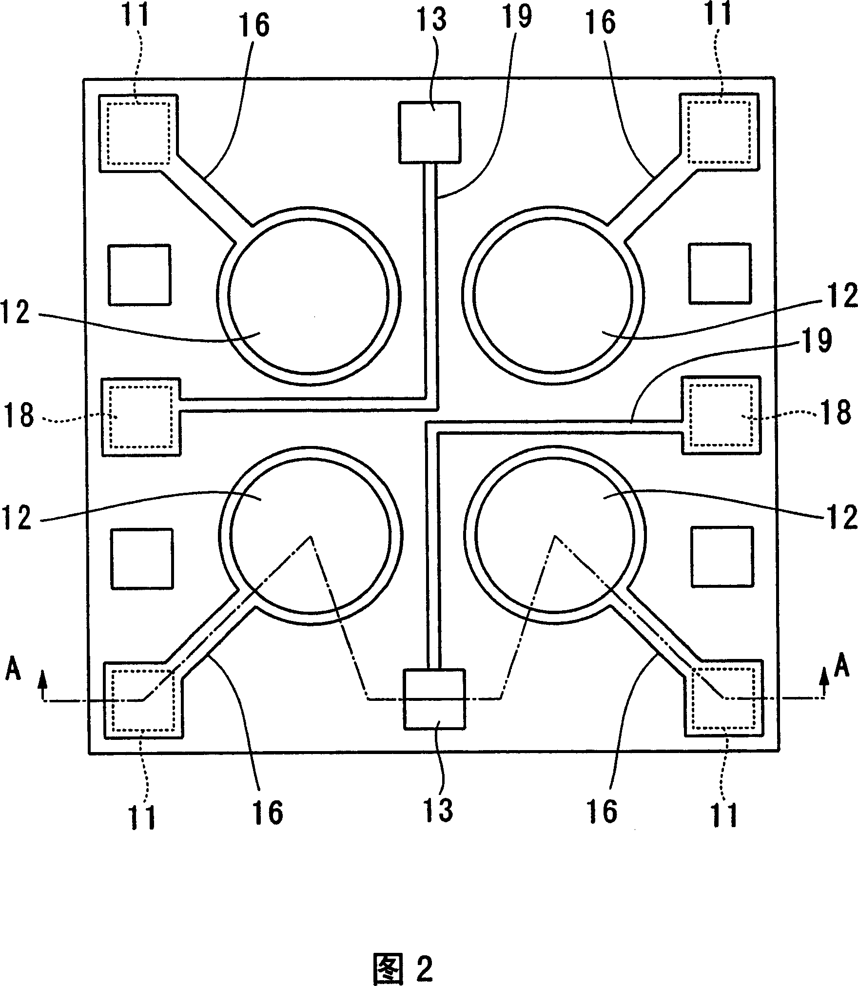
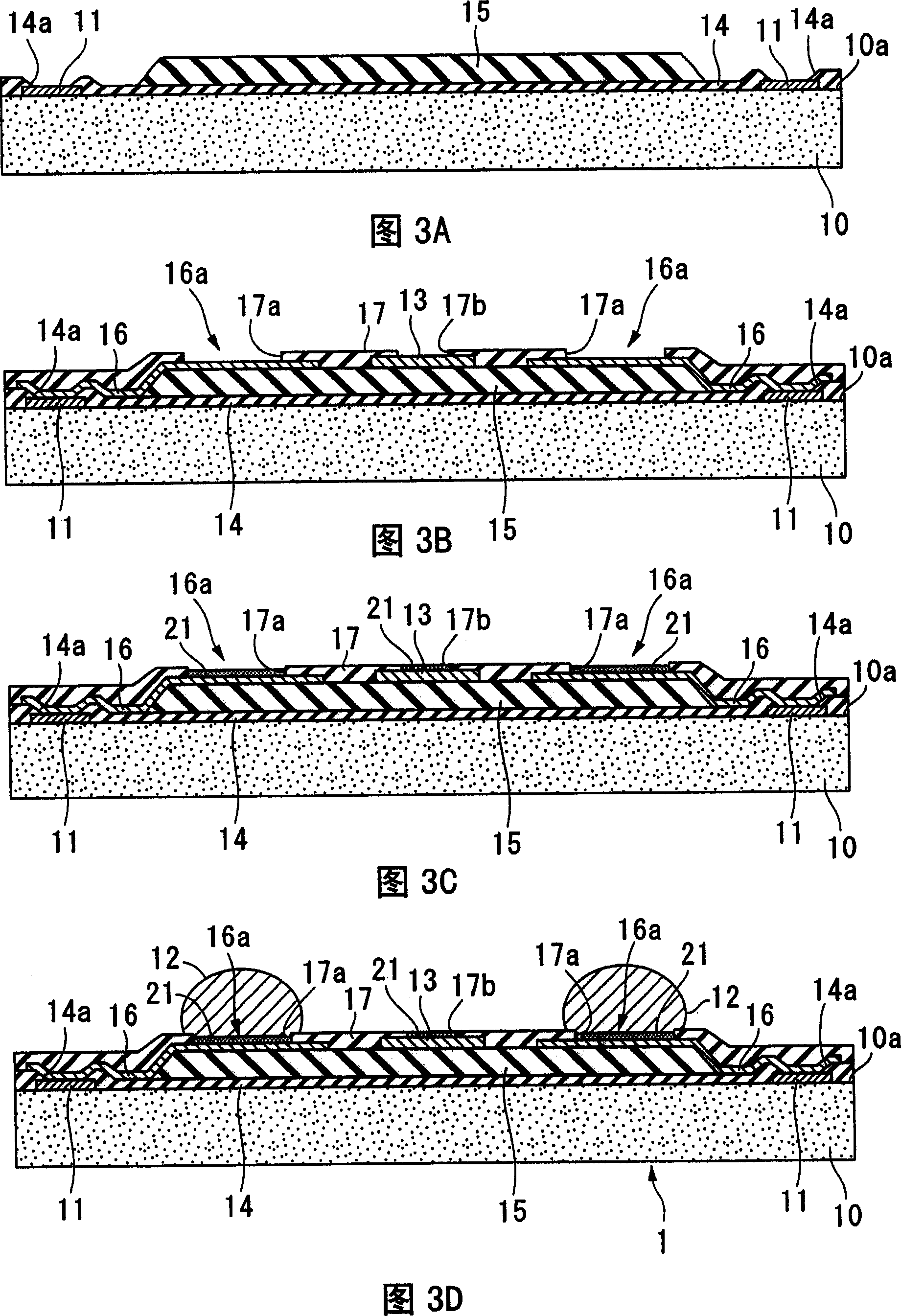
[0062] 1 and 2 are diagrams showing an embodiment of a semiconductor device of the present invention. In these figures, reference numeral 1 is a semiconductor device having a wafer-level CSP (W-CSP) structure.

[0063] In addition, the side sectional view of FIG. 1 is a sectional view along the line A-A in the schematic diagram of FIG. 2 .

[0064] As shown in FIG. 1 , a semiconductor device 1 includes a silicon substrate (semiconductor substrate) 10 , first electrodes 11 , external connection terminals 12 , and connection terminals 13 .

[0065] Here, an integrated circuit (not shown) including semiconductor elements such as transistors and memory elements is formed on a silicon substrate (...


PUM


Abstract

A semiconductor device, includes: a semiconductor substrate having an active face; a first electrode provided on or above the active face of the semiconductor substrate; an external connection terminal electrically connected to the first electrode and provided on or above the active face of the semiconductor substrate; and a connection terminal provided on or above the active face of the semiconductor substrate, wherein any of a gold plated film, a silver plated film, and a palladium plated film is formed on at least one of the external connection terminal and the connection terminal.

Description

technical field [0001] The present invention relates to a semiconductor device, a method of manufacturing the semiconductor device, an electronic component, a circuit board, and an electronic device. Background technique [0002] In order to mount semiconductor devices more densely, bare chip mounting is an ideal mounting method. [0003] However, bare chips have problems of difficulty in ensuring quality and troublesome handling. [0004] Therefore, conventionally, a semiconductor device to which CSP (Chip Scale / Size Package) is applied has been developed. [0005] In addition, especially in recent years, as described in Japanese Re-Explication No. 01 / 071805 and JP-A No. 2004-165415, the so-called "wafer-level CSP (W-CSP)" that forms CSP at the wafer level has been introduced. attention. [0006] In wafer-level CSP, a plurality of rewired semiconductor elements (integrated circuits) are formed in units of wafers, and then the wafer is cut to separate the plurality of sem...

Claims


Application Information

Patent Timeline
Patent Type & Authority Applications(China)
IPC IPC(8): H01L23/485H01L21/60H01L21/28
CPCH01L2924/01074H01L2924/01006H01L2924/01004H01L2924/01075H01L2924/01002H01L2924/01082H01L2924/01046H01L2924/04941H01L2924/01015H01L2924/01022H01L2924/01005H01L2924/01033H01L2924/01047H01L23/3114H01L2924/01079H01L24/13H01L2924/01013H01L2924/014H01L2924/14H01L2224/13099H01L2924/01078H01L2924/1461H01L2924/01023H01L2924/19043H01L24/10H01L2924/01029H01L2924/01024H01L24/02H01L24/03H01L24/05H01L2224/0236H01L2224/02377H01L2224/05001H01L2224/05008H01L2224/05022H01L2224/05024H01L2224/05124H01L2224/05139H01L2224/05144H01L2224/05147H01L2224/05155H01L2224/05164H01L2224/05166H01L2224/05171H01L2224/05184H01L2224/05548H01L2224/05569H01L2224/05571H01L2224/05639H01L2224/05664H01L2224/06131H01L2224/13H01L2224/13024H01L2924/00H01L2924/00014H01L23/48
Inventor 桥元伸晃
Owner SEIKO EPSON CORP
Why Eureka
Try Eureka