Optical identifying welding plate for printed circuit board and mfg. method

A printed circuit board, optical identification technology, applied in the direction of printed circuit components, electrical components to assemble printed circuits, etc., can solve the problems of poor identification point recognition effect, etc., to achieve the effect of high contrast

Active Publication Date: 2007-06-13
靖江德方科技服务有限公司
View PDF0 Cites 13 Cited by
  • Summary
  • Abstract
  • Description
  • Claims
  • Application Information

AI Technical Summary

Problems solved by technology

[0005] The invention overcomes the disadvantage of poor recognition effect on the recognition point in the prior art, and provides an o

Method used


Image

  • Optical identifying welding plate for printed circuit board and mfg. method
  • Optical identifying welding plate for printed circuit board and mfg. method

Examples


Embodiment 1

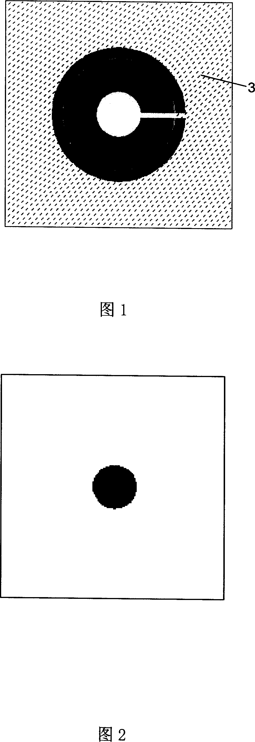
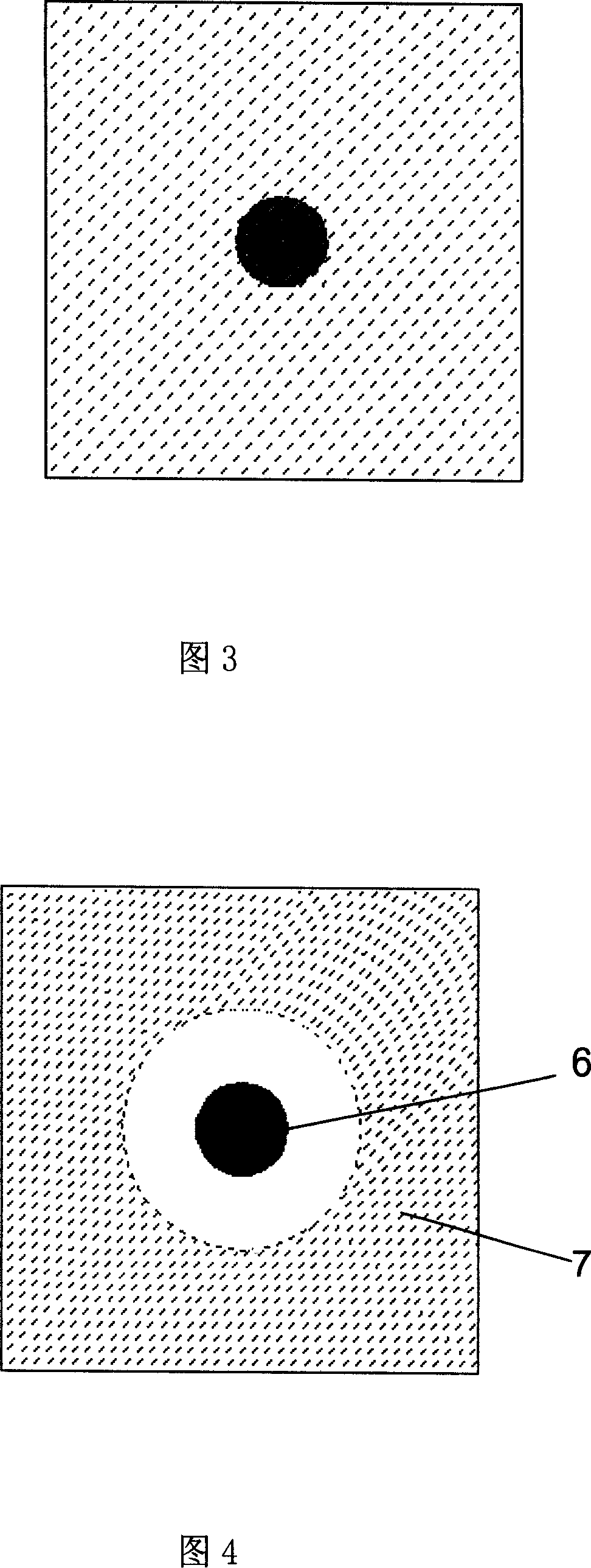
[0015] Embodiment 1: An optical identification pad of a printed circuit board, including a pad located on a printed circuit board, and an optical identification point on the pad, and the contrast between the optical identification point and the surrounding is different, so The above-mentioned optical recognition point is an etching point, and there is a solder resist area opening around the recognition point on the pad, and there is a plating layer in the solder resist opening area, and the plating layer can be a gold-plated layer. The etching point may be circular, the gold-plated layer is circular, and the welding pad is made of copper foil.

Embodiment 2

[0016] Embodiment 2: A method for manufacturing an optical identification point of a flexible printed circuit board, comprising the following steps: 1) removing a circular area on the copper foil to form an etching point, 2) performing solder resist on the pad, and the solder resist area An opening is formed around the identification point, and a plating layer is plated on the opening area of ​​the solder resist around the identification point, and the plating layer is a gold-plated layer.

[0017] A double-sided flexible printed circuit board product needs to be equipped with various electronic components such as capacitors, resistors, connectors, and BGAs. As shown in Figure 2 and Figure 4, when making the circuit of the flexible printed circuit board, a circular mark (mark) point 6 is first etched on the copper foil. At this time, the mark (mark) point 6 is black, and then the copper foil is etched For solder masking of the foil, it is necessary to design a solder mask open...


PUM


Abstract

This system includes: (1) the soldering plates (SP) residing on the printed circuit board (PCB), (2) the photo recognition points (PRP), which contrast differs from ambient, (3) the etch points (EP) remained from removing PRP on SP, (4) the soldering resistance (RS) area with openings around PRP, and (5) the plating layer on this RS opening area. This invention also offers a manufacture method for the PRP on a flexible PCB. It includes steps of 1) etching a PRP on SP, 2) making RS on SP, making openings around PRP on RS area, and then plating the opening area. On the flexible PCB made by this way, the color contrast between PRP and the ambient is rather high. The shape of PRP is round. Due to the good photo recognition effect, the surface stick installation machine can accurately orientate with the aid of photo recognition.

Description

【Technical field】 [0001] The invention relates to an optical identification pad of a printed circuit board and a manufacturing method thereof, in particular to an optical identification pad of a flexible printed circuit board and a manufacturing method thereof. 【Background technique】 [0002] Before the flexible printed circuit board (FPC) is applied to electronic products, it needs to carry various electronic components such as capacitors, resistors, ICs and connectors. At present, surface mount technology (SurfaceMounting Technology, referred to as SMT) is mostly used to solder electronic components on flexible printed circuit boards. And more and more surface mount machines use optical recognition methods to locate the position to be soldered on the flexible printed circuit board. The principle of optical recognition is: the higher the contrast between the recognition point on the flexible printed circuit board and the surrounding color, the better the recognition effect...

Claims


Application Information

Patent Timeline
IPC IPC(8): H05K1/02H05K3/34
Inventor 欧阳小庆
Owner 靖江德方科技服务有限公司
Why Eureka
Try Eureka