X-ray detecting method for printed circuit board defect

A printed circuit board, light detection technology, used in electronic circuit testing, non-contact circuit testing, material analysis using radiation, etc. and other problems to achieve high test coverage, improve first pass rate, and shorten preparation time.

Inactive Publication Date: 2007-06-27
SOUTH CHINA UNIV OF TECH
View PDF0 Cites 25 Cited by
  • Summary
  • Abstract
  • Description
  • Claims
  • Application Information

AI Technical Summary

Problems solved by technology

However, the AOI system also has shortcomings, such as the inability to detect circuit errors, and the detection of the internal conditions of invisible solder joints is also powerless
[0008] The prior art has the following deficiencies in the detection technology of printed circuit boards: it is impossible to detect invisible solder joints, such as ball grid array packaging BGA, etc., s...

Method used


Image

  • X-ray detecting method for printed circuit board defect
  • X-ray detecting method for printed circuit board defect
  • X-ray detecting method for printed circuit board defect

Examples


Embodiment Construction

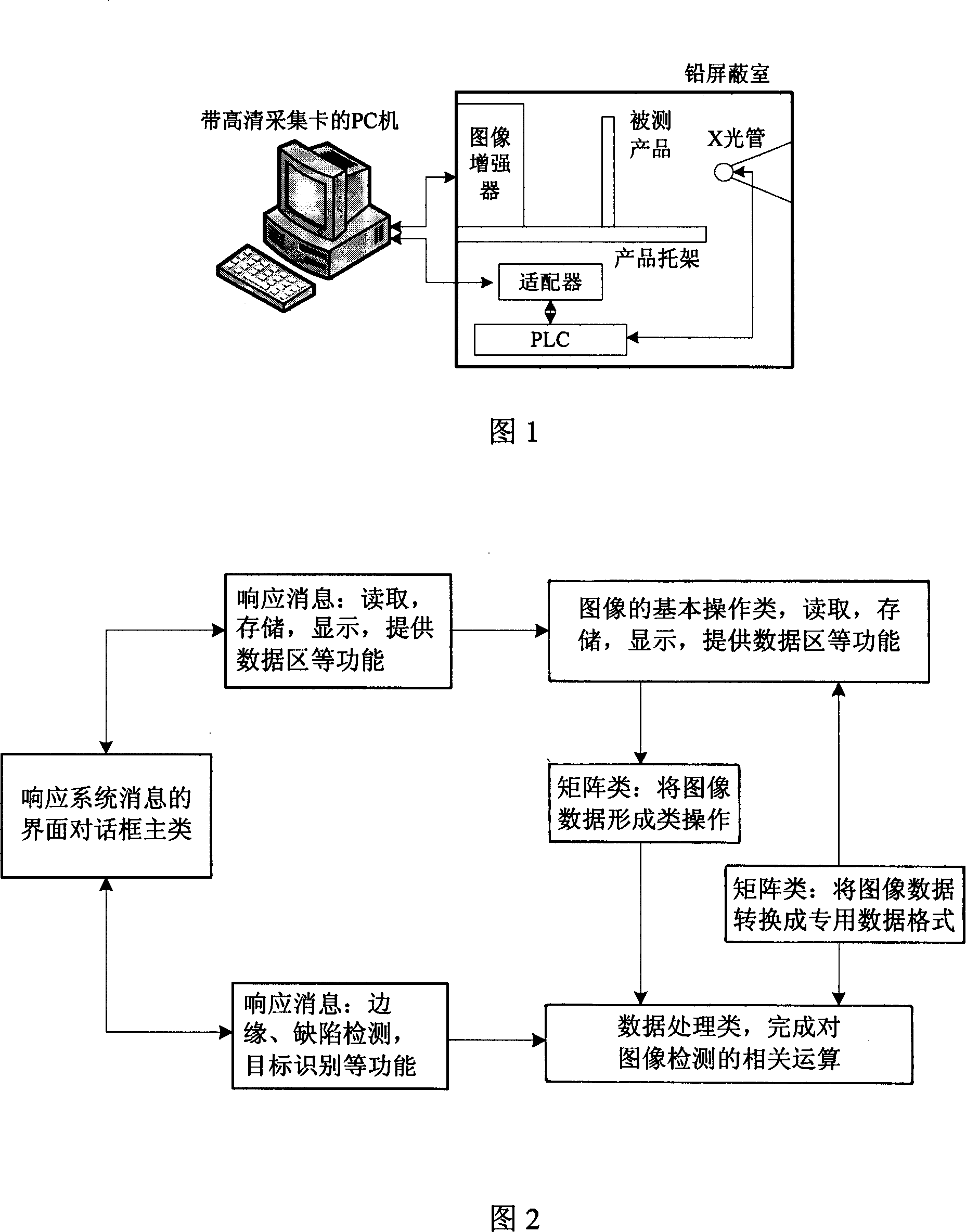
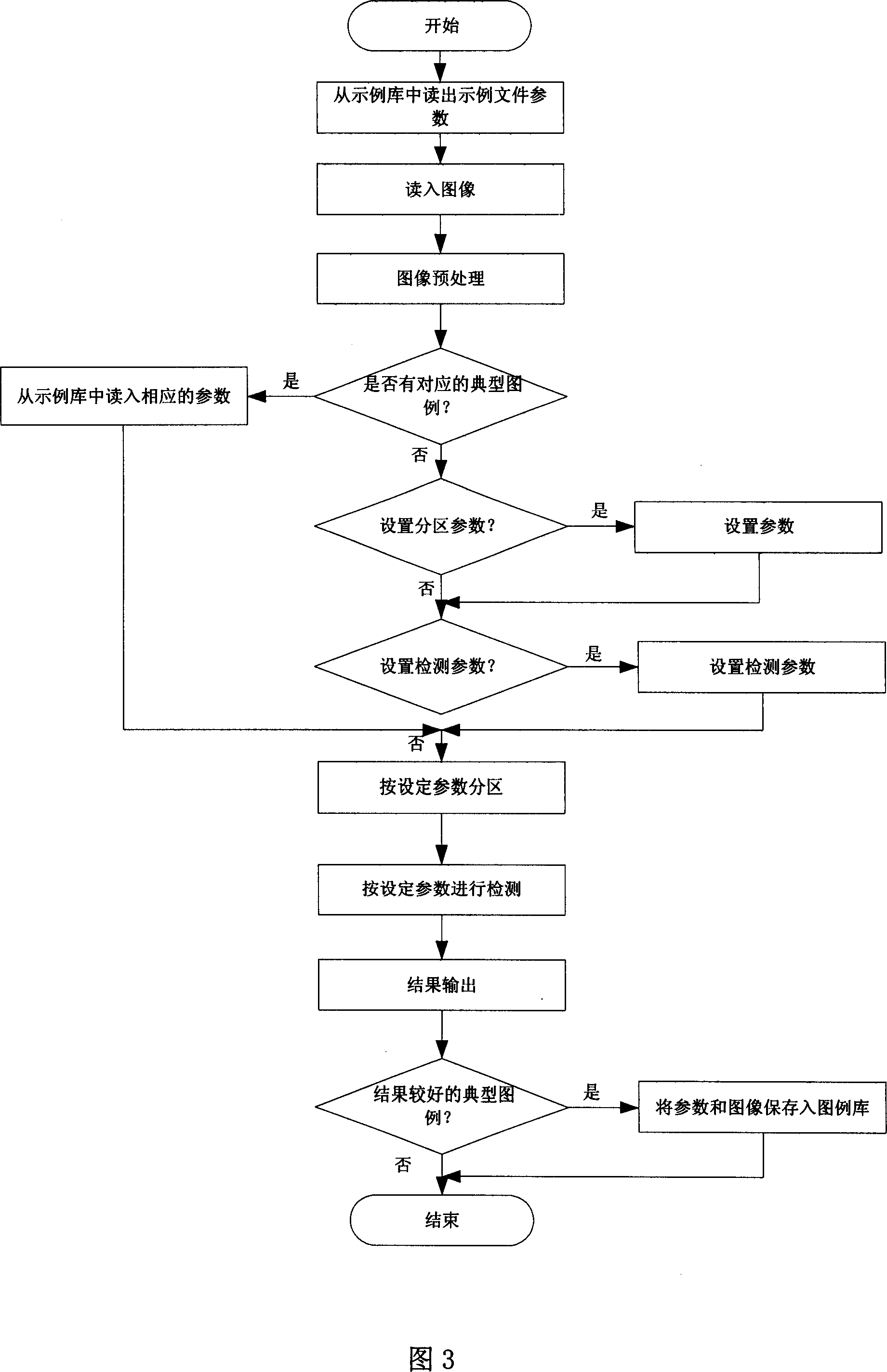
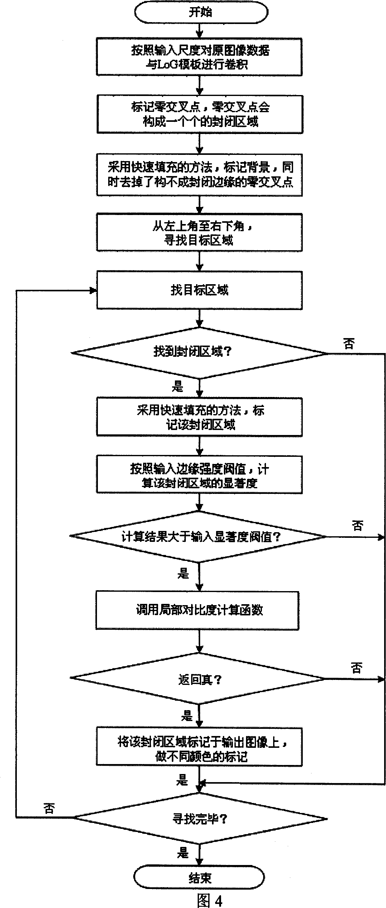
[0050] Using X-ray inspection, the internal defects of the printed circuit board are reflected as a flat image. The present invention specifically describes the method and system for automatic analysis and detection of internal defects of printed circuit boards through the analysis and identification of X-ray images of printed circuit board defects. The method and system of the present invention can be used to analyze and identify any Acquired images and graphics of internal defects in printed circuit boards.

[0051] The method and system of automatic analysis and detection of printed circuit board internal defects of the present invention can be realized by software, hardware or a combination of software and hardware, such as writing system processing software with Fortran and C language on a general-purpose computer to realize the method of the present invention, or using General-purpose or special-purpose DSP and a special-purpose accelerated processor on a general-purpose...


PUM


Abstract

The intelligent analysis method, the intelligent system, and method for controlling position of X light source are in use for checking products of print circuit board (PCB). Defect recognition algorithm raises accuracy of recognition, and lowers erroneous judgment of false defect. Through user's main threaded, threaded of background operator, and monitoring threaded of serial port, the disclosed intelligent system at PC end, as well as PLC communication and control multithreading implements coordinational synchronization between PC intelligent system and PLC. Since penetrability of X ray, percentage of coverage for detecting defective workmanship of PCB by system is raised greatly.

Description

technical field [0001] The invention relates to a detection method for defects of an assembled printed circuit board (PCBA), in particular to an X-ray detection method for defects of a printed circuit board. Background technique [0002] With the rapid development of electronic technology, the miniaturization of packaging and the high density of assembly, as well as the continuous emergence of various new packaging technologies, the requirements for the quality of electronic assembly are also getting higher and higher. Therefore, higher requirements are put forward for inspection methods and techniques. At present, there are many kinds of testing technologies used in the field of electronic assembly testing, such as manual visual inspection (MVI), online testing (ICT), automatic optical testing (AOI), automatic X-ray testing (AXI), and functional testing (FT). Wait. These detection methods have their own advantages and disadvantages. [0003] Different testing techniques ...

Claims


Application Information

Patent Timeline
IPC IPC(8): G01N23/18G01R31/308
Inventor 黄茜
Owner SOUTH CHINA UNIV OF TECH
Why Eureka
Try Eureka