Vertical boat and vertical heat processing apparatus for semiconductor process

A semiconductor, vertical technology, applied in semiconductor/solid-state device manufacturing, lighting and heating equipment, furnace types, etc., can solve problems such as cracks and wafer scars

Inactive Publication Date: 2007-07-04
TOKYO ELECTRON LTD
View PDF4 Cites 15 Cited by
  • Summary
  • Abstract
  • Description
  • Claims
  • Application Information

AI Technical Summary

Problems solved by technology

The technology disclosed in this bulletin is based on the viewpoint that: in the ring-shaped wafer boat, due to the contact be

Method used


Image

  • Vertical boat and vertical heat processing apparatus for semiconductor process
  • Vertical boat and vertical heat processing apparatus for semiconductor process
  • Vertical boat and vertical heat processing apparatus for semiconductor process

Examples


Embodiment Construction

[0042] The inventors of the present invention have studied problems related to vertical boats for wafer heat treatment that occur in vertical heat treatment apparatuses during the development of the present invention. As a result, the present inventors have made the findings described below.

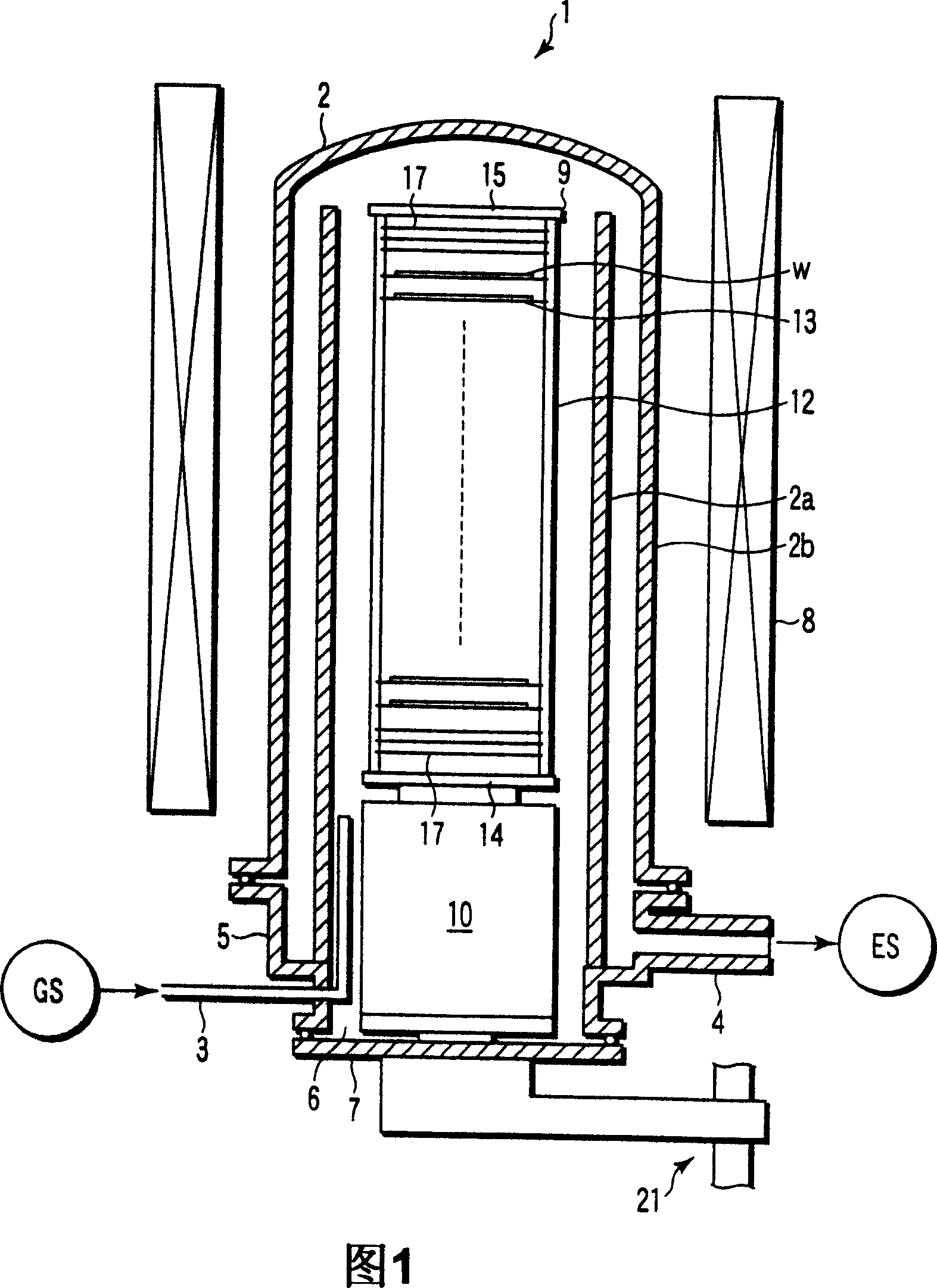
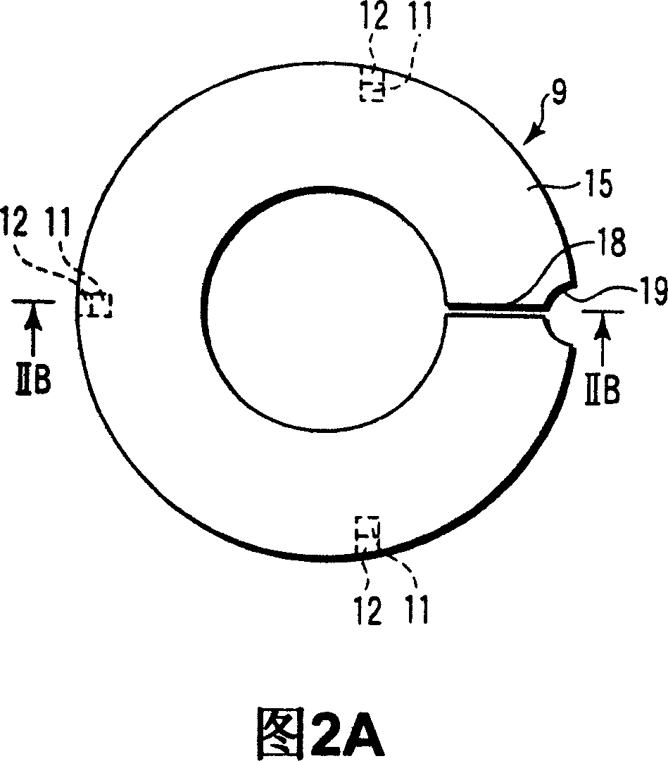
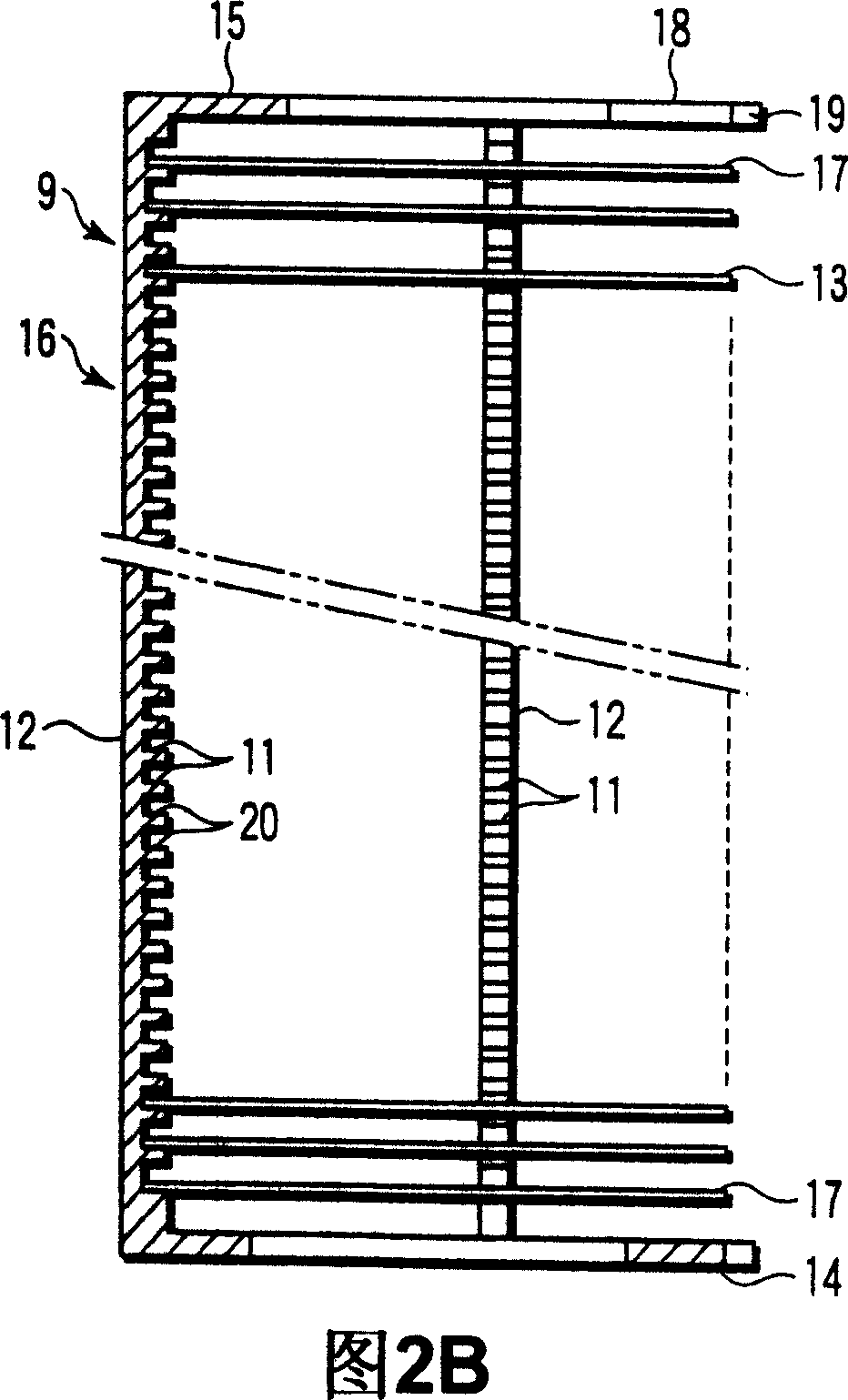
[0043] FIG. 8A is a cross-sectional view explaining a problem caused by self-weight stress of a wafer when a vertical wafer boat is used. FIG. 8B is a cross-sectional view explaining a problem caused by thermal expansion of a wafer when a vertical wafer boat is used. In this vertical boat, the upper surface 13 a of the support plate 13 is formed in a horizontal state. If the wafer W is placed on the support plate 13, as shown in FIG. 8A, the central part of the wafer W will be bent downward due to the stress of its own weight. As a result, stress concentration occurs at the portion of the wafer W corresponding to the inner peripheral portion of the support plate 13 (indicated by a x ma...


PUM


Abstract

A vertical boat for a semiconductor process is used for supporting target substrates during a heat process performed on the target substrates. The vertical boat includes struts fixed to a fixing member and arrayed at intervals in an annular direction, and fin portions formed on each of the struts at intervals in a vertical direction. Annular support plates are configured to respectively support the target substrates. Each of the annular support plates is held by corresponding fin portions of the struts located at the same height. Each of the annular support plates has an upper surface inclined inwardly downward with inclination set to agree with deformation of a corresponding one of the target substrates caused during the heat process, so that the upper surface comes into plane contact with a bottom of the target substrate during the heat process.

Description

[0001] Cross-references to related applications [0002] This application is based on and claims priority from prior Japanese Patent Applications No. 2005-378890 filed on December 28, 2005 and No. 2006-283886 filed on October 18, 2006, the entire contents of which are hereby incorporated by reference For reference. technical field [0003] The present invention relates to a vertical wafer boat and a vertical heat treatment apparatus for semiconductor processing for processing substrates such as semiconductor wafers. The term "semiconductor processing" here refers to the process of forming a semiconductor wafer in a prescribed pattern on a substrate to be processed such as a semiconductor wafer or a glass substrate used in a flat panel display (FPD) (Flat Panel Display) of a liquid crystal display LCD (Liquid Crystal Display). Layers, insulating layers, conductive layers, etc., so as to manufacture semiconductor elements or components including wiring and electrodes connected ...

Claims


Application Information

Patent Timeline
IPC IPC(8): H01L21/673H01L21/67H01L21/324H01L21/22H01L21/00F27D5/00F27B17/00
Inventor 谷裕一
Owner TOKYO ELECTRON LTD
Why Eureka
Try Eureka